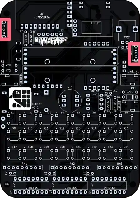
Build Order
- Pot
- Pot Cap 102/1nF
- 3.5mm Jacks
- PCM1808
- OLED
- PCM5102
- SD Module
- MAX98357A
- Resistors
- Caps 104/100nF x4
- Diode 1N4148
- Diode SB240
- 6N138
- MIC
- 74HC165 x 3
- Resistor Networks
- Small Slide Switches
- Large Slide Switch
- Tactile Switches x 24
- Power Module
- Battery Holder
- Speaker
- Enclosure
TOP
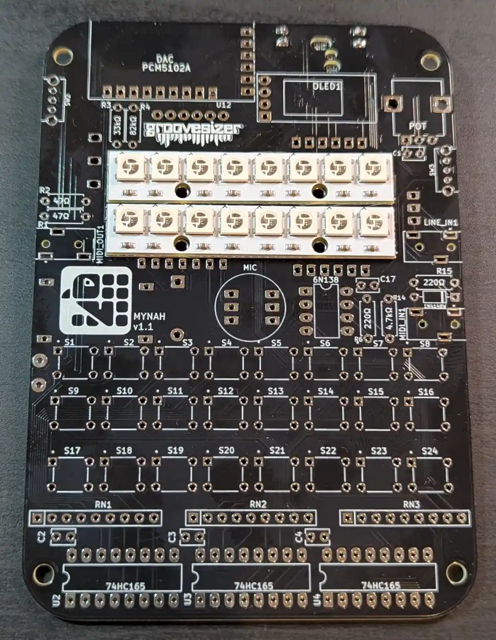
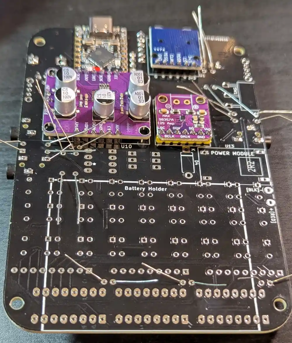
Here’s the top of the board as you receive it. The neopixel sticks have been pre-soldered.
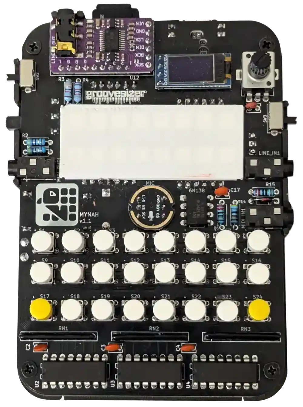
The top fully built.
BOTTOM
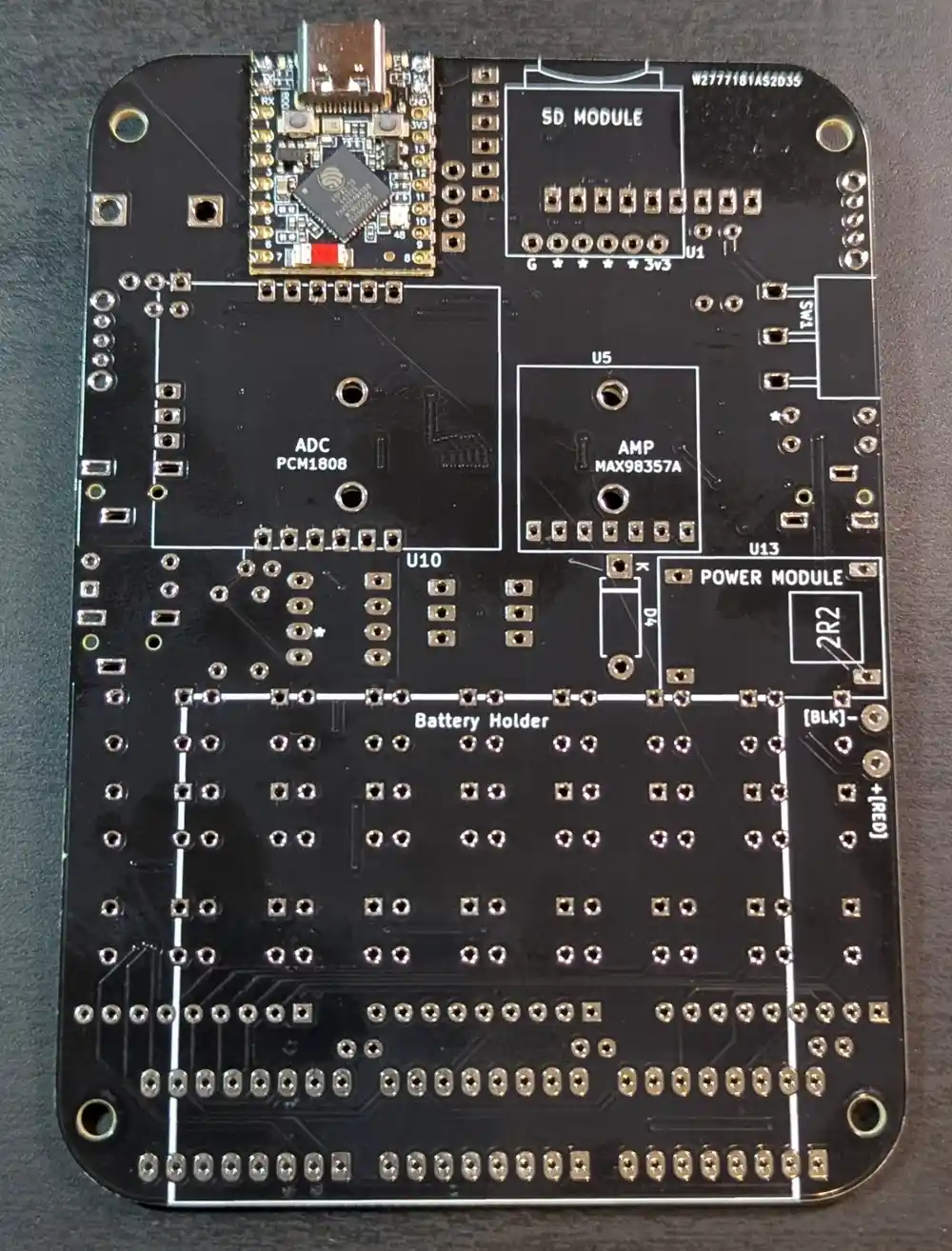
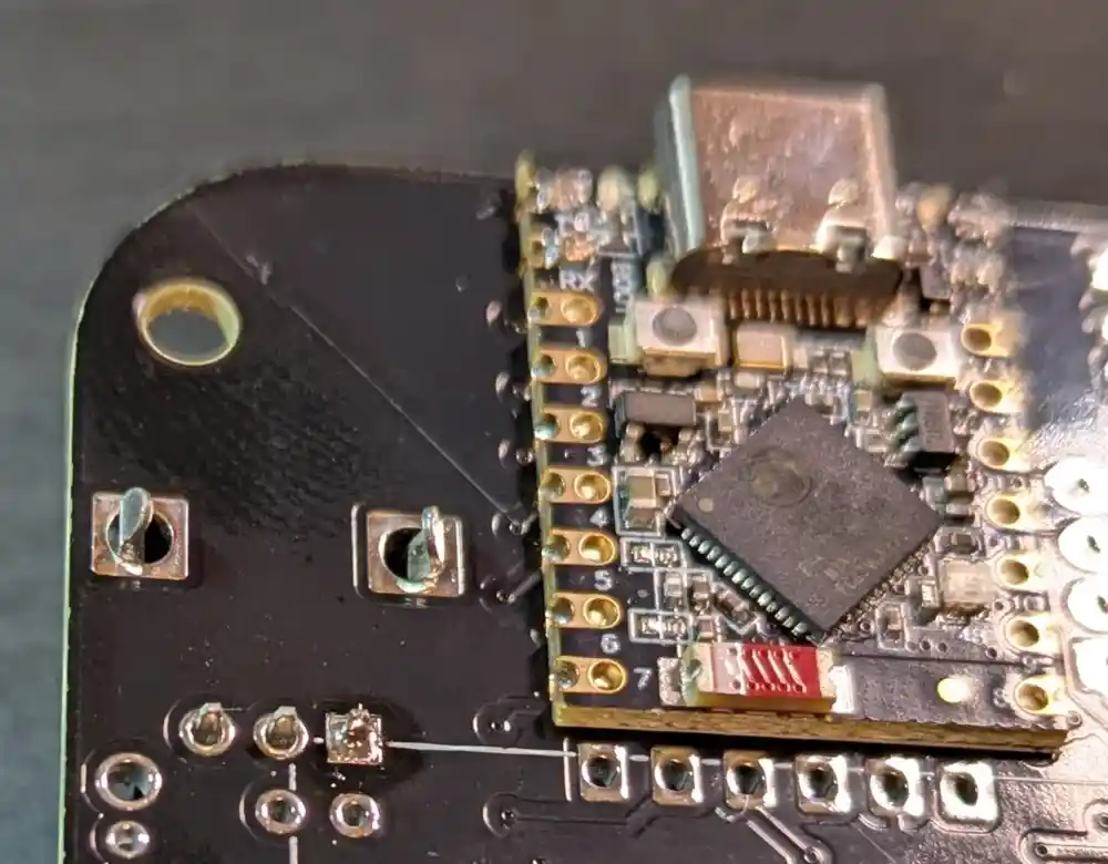
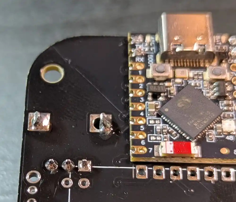
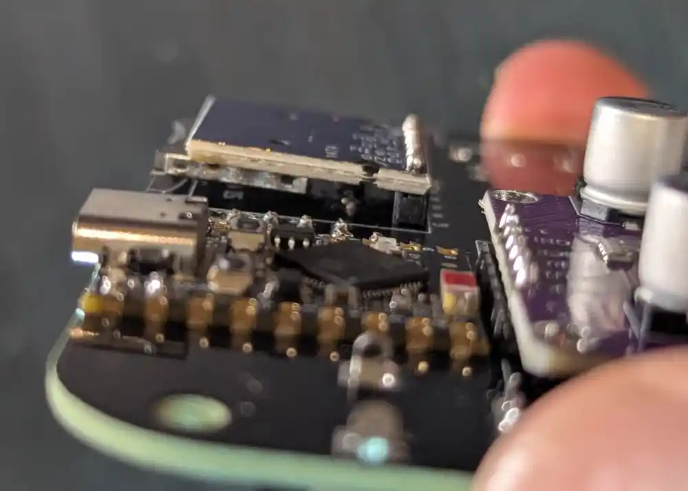
And here’s the bottom. The ESP32-S3 SuperMini board (the Mynah’s brain) has been pre-soldered. In addition to the pads on the sides of the microcontroller PCB, there are also a number of blind pads on the bottom, requiring the microcontroller to be soldered using a hot plate.
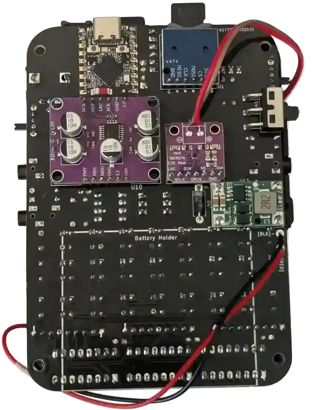
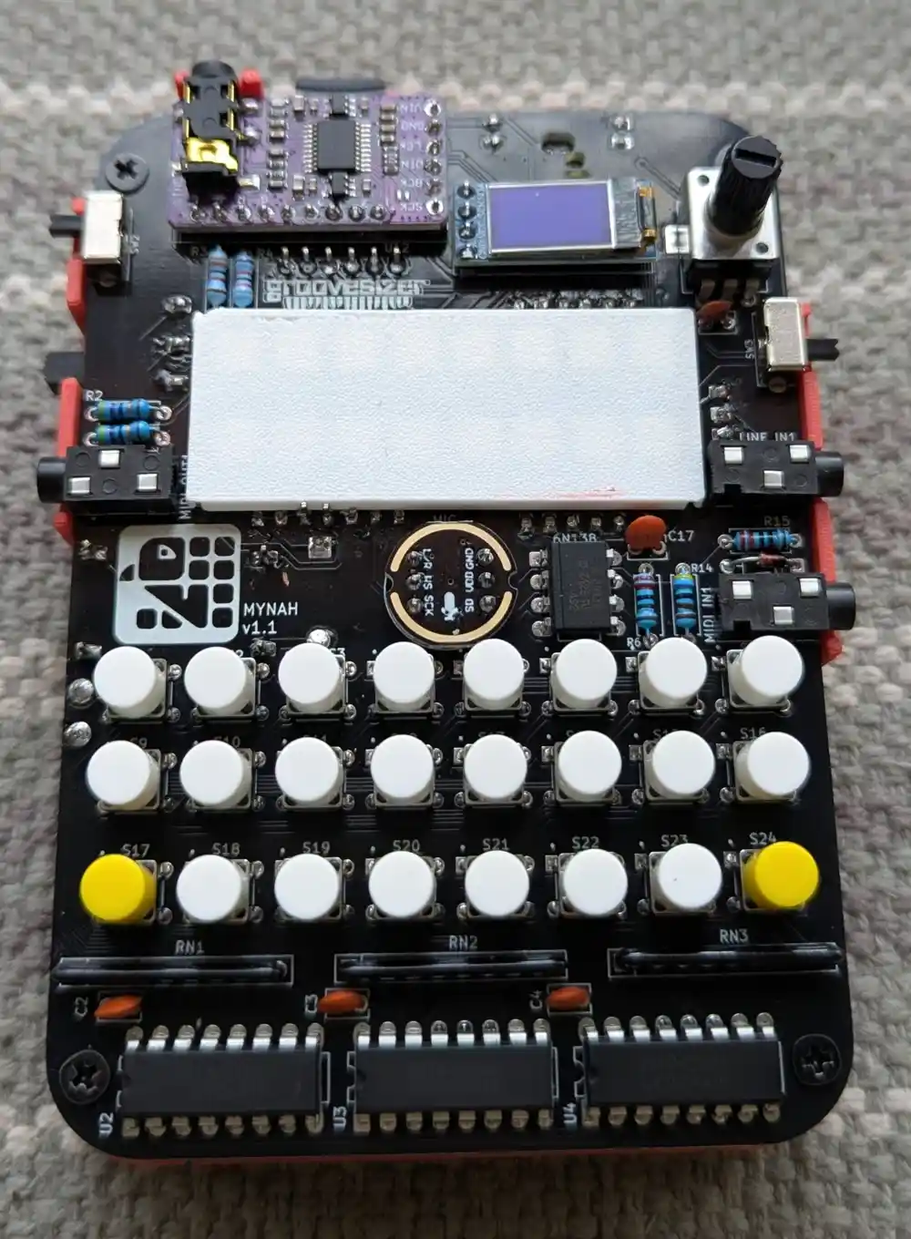
The fully built bottom.
Floyd Steinberg’s video on the Mynah follows these build instructions closely and is a great additional reference. Thank you, Floyd!
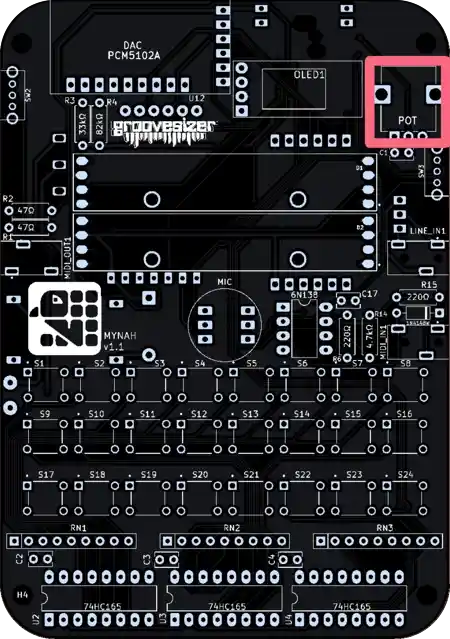
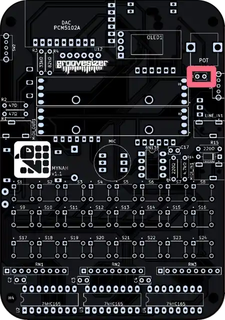
1. Potentiometer
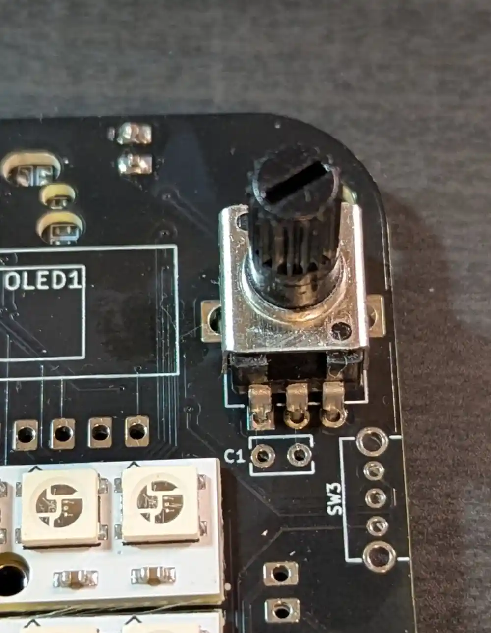
1.1 Potentiometer
We’ll start by inserting the potentiometer (marked POT) on the top of the board.
Commonly, tall components like this would be soldered last to make it easier to flip the PCB and solder components without them falling out. In this case, however, some of the potentiometer pins will be hard to reach unless we solder the pot first.
1.2 Potentiometer (Cont.)
Flip the board over, then solder one leg first. With one leg soldered, check the positioning of the pot. You can heat the single solder joint and straighten the pot if required. Once more than one joint has been soldered, it becomes very hard to fix positioning.
1.3 Potentiometer (Cont.)
With the potentiometer straight, now solder the remaining pins.
2. Capacitor (1nF)
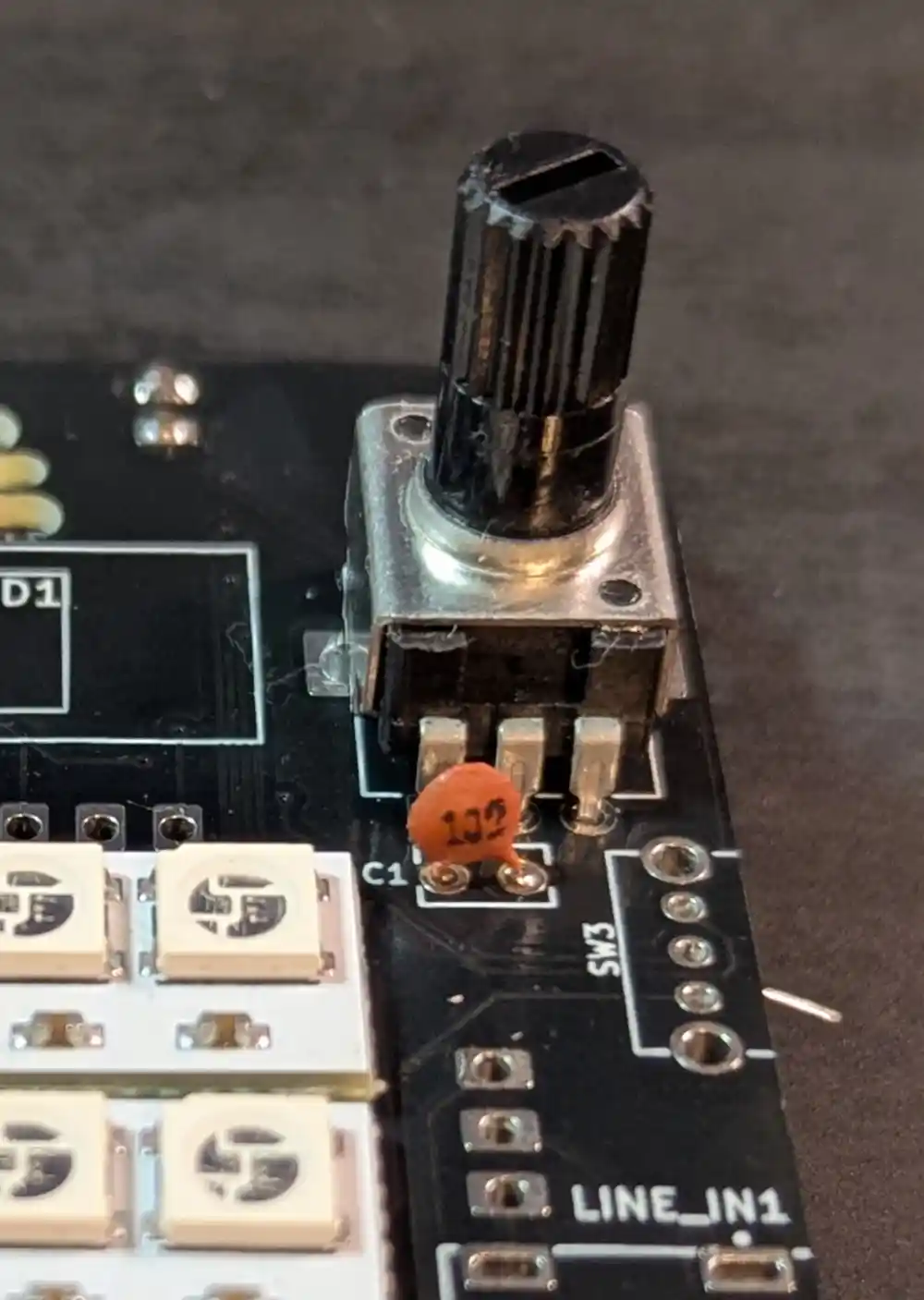
2.1 Capacitor (1nF)
Let’s insert the ceramic 1nF capacitor (marked 102 on the body and C1 on the PCB) on the front of the board, just under the potentiometer.
The cap is non-polarized, so it can go in either way around. The cap helps filter out noise so we can get clean and consistent readings from the potentiometer.
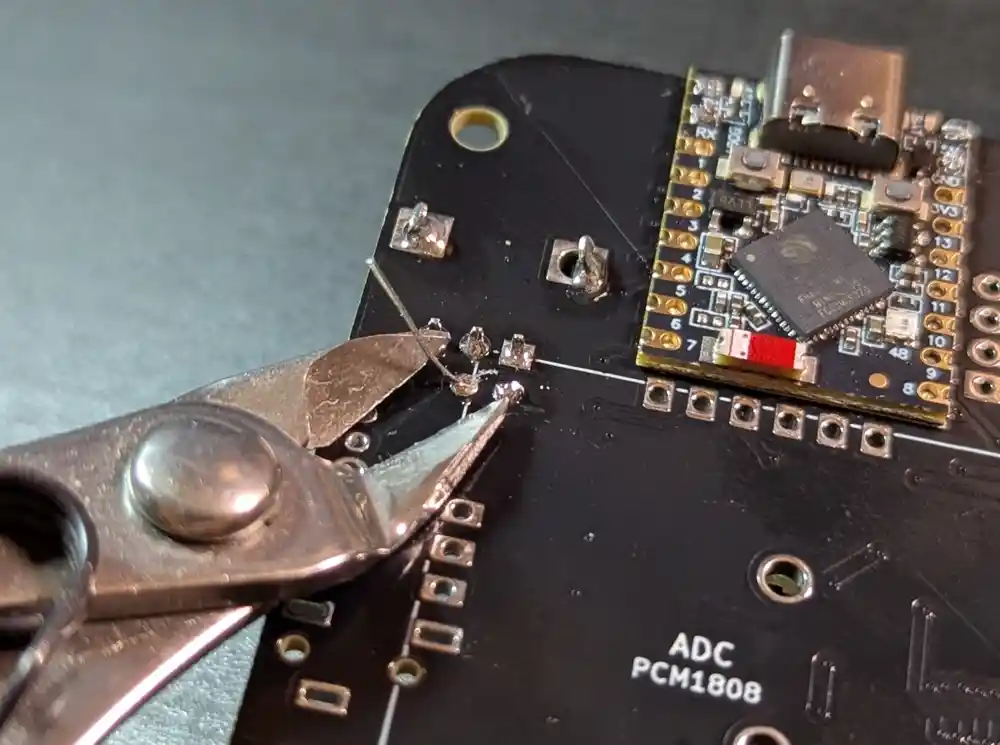
2.2 Capacitor (1nF – Cont.)
Let’s flip the board over, solder the leads, then snip off the excess with our edge cutters. Double-check the solder joints at this point, as they will sit under the PCM1808 PCB later on and will be hard to reach.
3. Jacks (3.5mm)
3.1 Jacks (3.5mm)
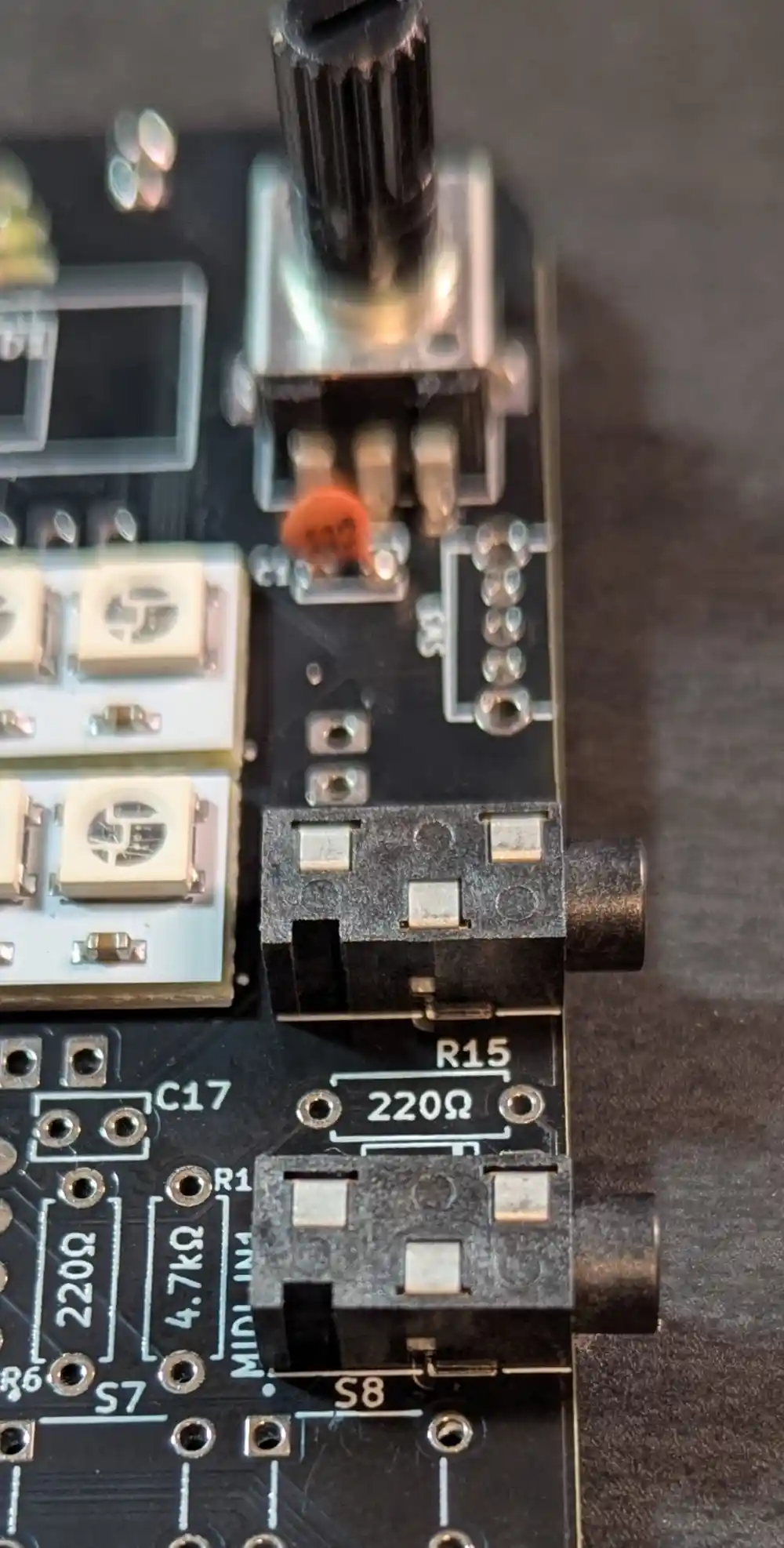
Back on the front of the board, let’s insert the 2x 3.5mm jacks on the right side of the board.
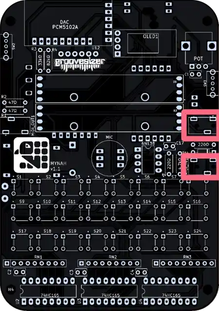
The one closest to the potentiometer is our line input, and the one below it is the MIDI input. They’re marked MIDI_IN1 and LINE_IN1 on the PCB.
3.2 Jacks (3.5mm – Cont.)
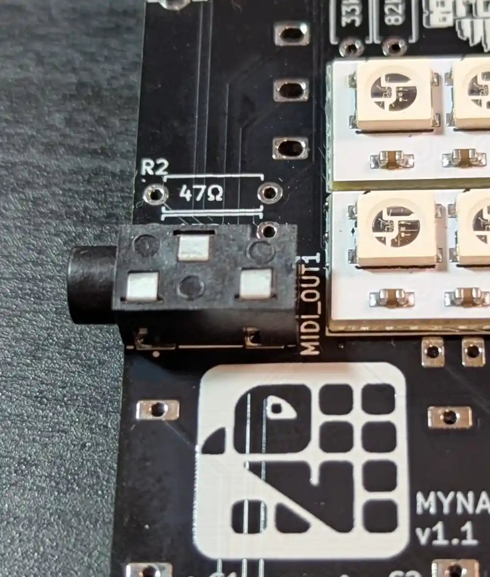
Let’s also add the jack on the left side of the board. Now let’s flip the board and solder all three jacks. They’ll want to fall out, so I solder them on the edge of my desk with the potentiometer hanging off. You can also hold them down with sticky tape if you like. Either way, it’s important to do that trick with soldering one leg first, ensure the jacks are flush with the board and straight before then soldering the remaining legs.
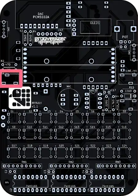
This is our MIDI output jack appropriately marked MIDI_OUT1 on the PCB.
4. PCM1808 Module
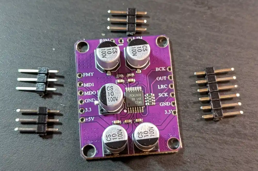
4.1 PCM1808 Module
The PCM1808 module handles audio arriving via our line input – it’s an analog-to-digital convertor (ADC) that converts analog audio into digital I2S signals. First, we want to snip the headers to the correct lengths. The supplied headers are only enough for the two long rows. For the row of 3 pins, you can grab some from the header supplied with the power module – that’s the module we will add in step 20 (we only need 4 pins there).
4.2 PCM1808 Module (Cont.)
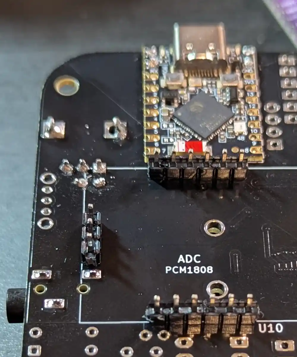
Next, we insert the headers on the bottom of the board, just below the ESP32 – nothing to solder just yet.
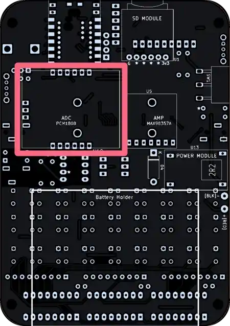
The PCB footprint is marked ADC PCM1808.
4.3 PCM1808 Module (Cont.)
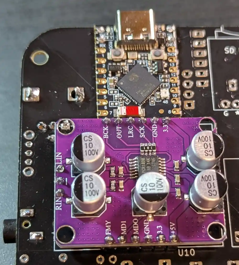
Then we place the module on the headers as pictured, and solder all 15 pins on this side of the board, ensuring that the module’s PCB is flush with the headers as we go.
4.4 PCM1808 Module (Cont.)
After flipping the board and soldering the module’s pins on the top side of the board, we can snip off the excess with our edge cutters. This will give us more room to maneuver later.
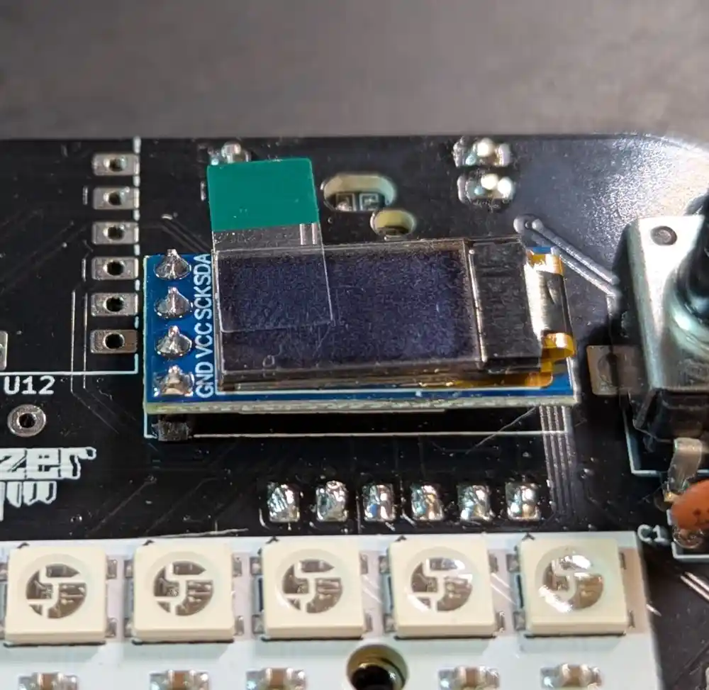
5. OLED Display
5.1 OLED Display
We insert the OLED and its header on the top of the board next to the potentiometer as pictured.
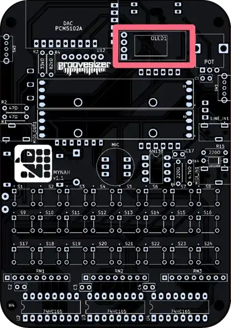
It’s marked as OLED1 on the board.
5.2 OLED Display (Cont.)
Let’s solder the OLED to its header on the top of the board, ensuring that the OLED PCB is flush against the header. Since it’s not soldered to the main PCB yet, it’s going to lean to the right side.
5.3 OLED Display (Cont.)
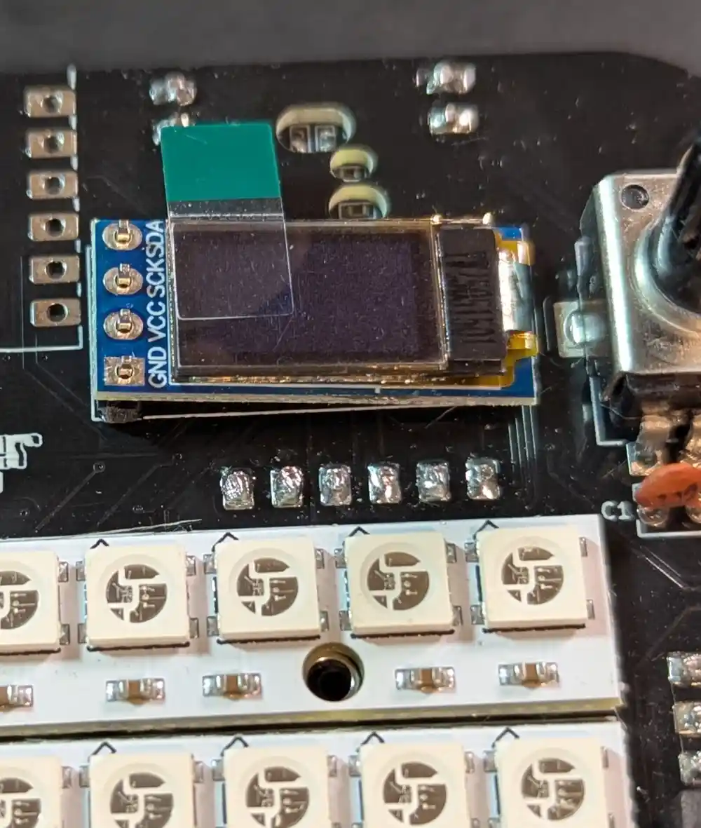
Next, we flip the board and solder first one pin, so we can ensure the OLED is straight and standing up (ie. with the header of the board flush against the main PCB, the right side of the OLED should now be hanging in the air).
5.4 OLED Display (Cont.)
Here’s what we expect to see on the top of the board. The OLED PCB is so light that there’s no issue with it only being anchored on the left side.
5.5 OLED Display (Cont.)
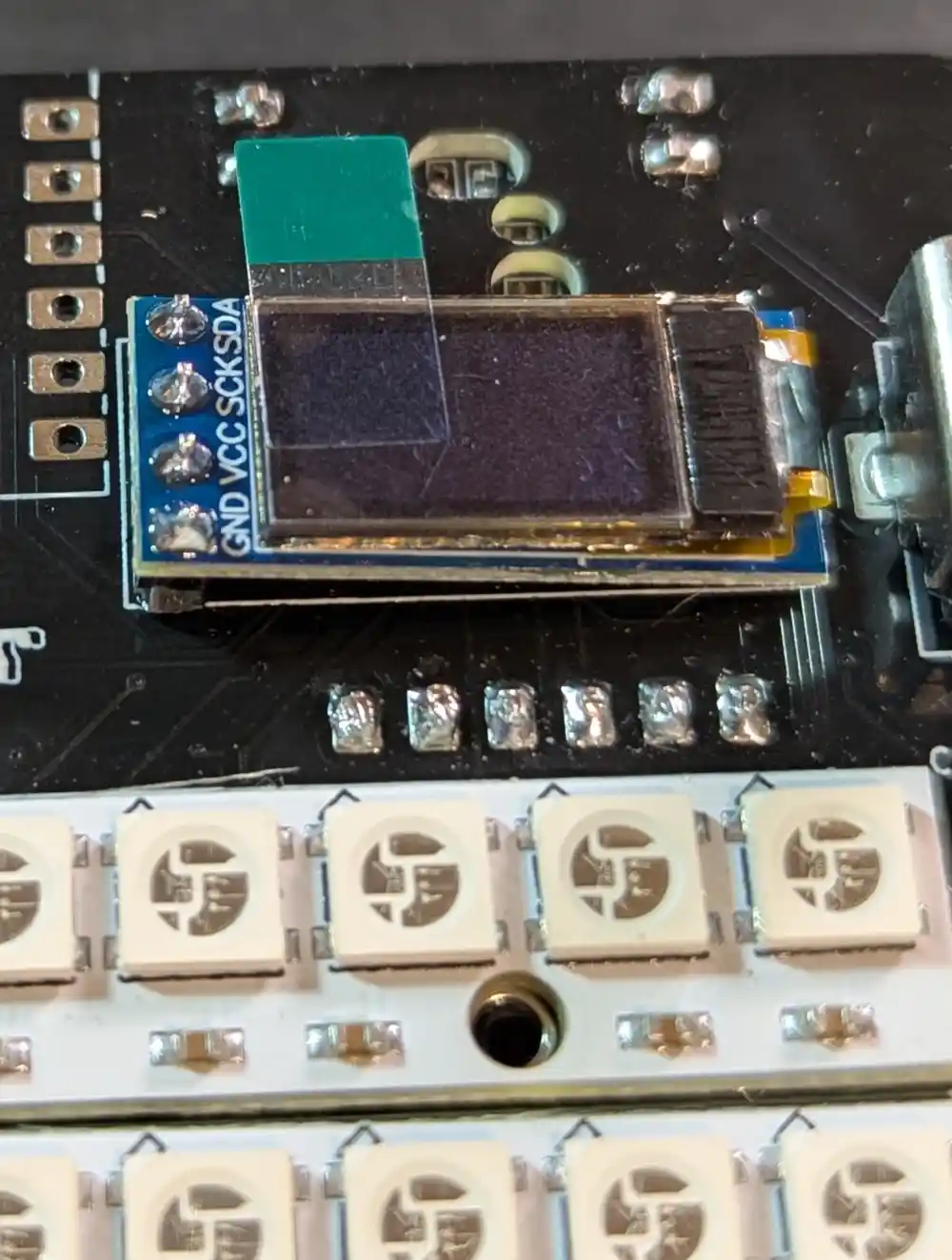
With the positioning and alignment confirmed, we can now solder the remaining legs and snip them off. Take care here since we don’t want to damage the microcontroller in this step.
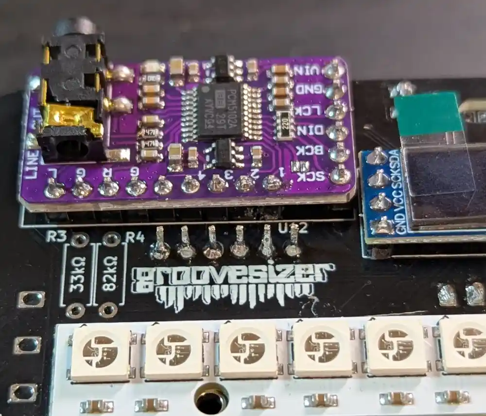
6. PCM5102 Module
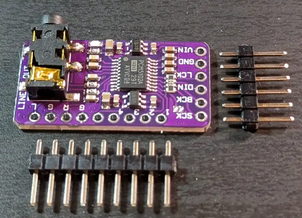
6.1 PCM5102 Module
The PCM5102 converts digital I2S audio signals from the microcontroller into high-quality analog signals to drive the Mynah’s output. As with the PCM1808, we want to cut the provided headers to the correct length.
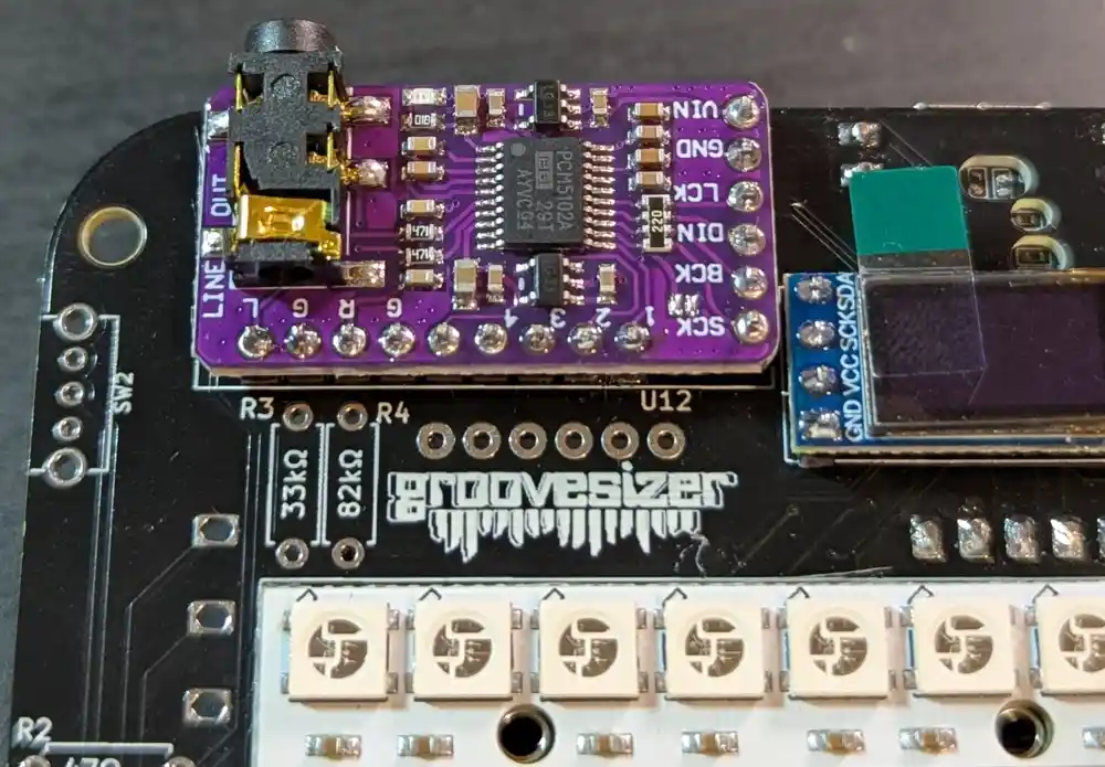
6.2 PCM5102 Module (Cont.)
We insert it on the top of the board, then solder the pin headers to the PCM5102’s PCB.
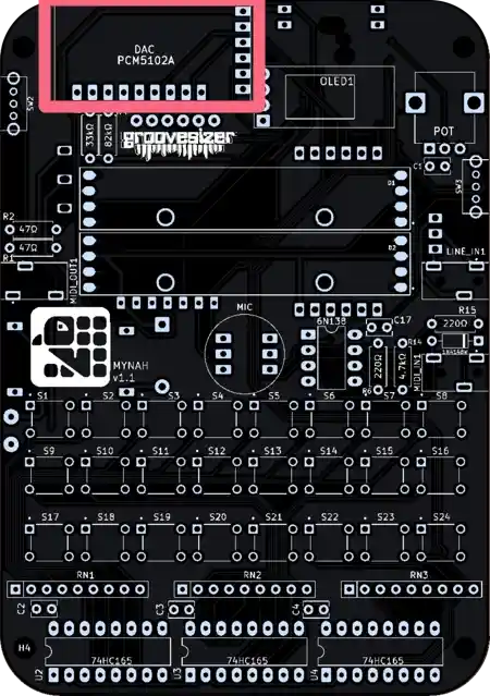
The footprint is labeled DAC PCM5102A on the PCB.
6.3 PCM5102 Module (Cont.)
To solder the module on the bottom of the board, you may want to prop it up with the handle of your edge cutters to prevent it from falling out. Again, one leg first, ensure it’s flush and straight, then solder the remaining legs. The alignment is important as the audio ouput jack needs to fit the hole in the enclosure later.
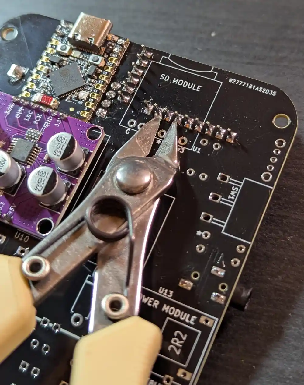
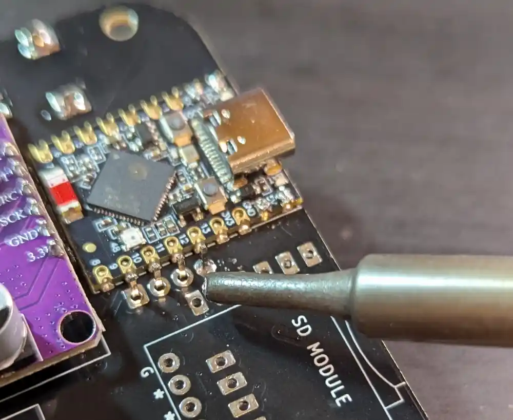
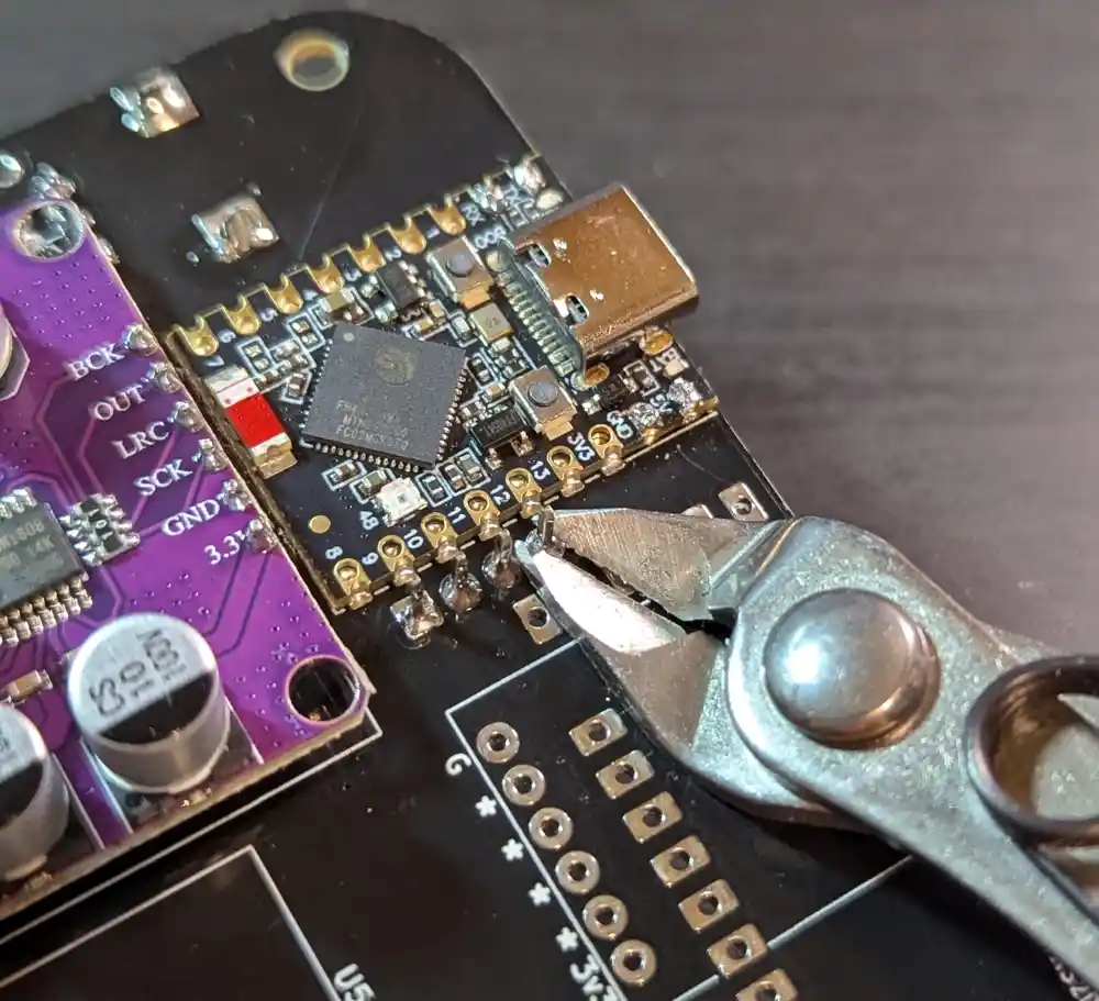
6.4 PCM5102 Module (Cont.)
We need to trim down the excess leads here, especially the ones that will be located beneath the SD module. Inspect the solder joints here carefully, since they will be impossible to reach once the SD module is soldered. It can’t hurt to reflow the solder one last time on any suspicious looking pins.
All nicely trimmed, though I could have cleaned the flux here with some isopropyl alcohol.
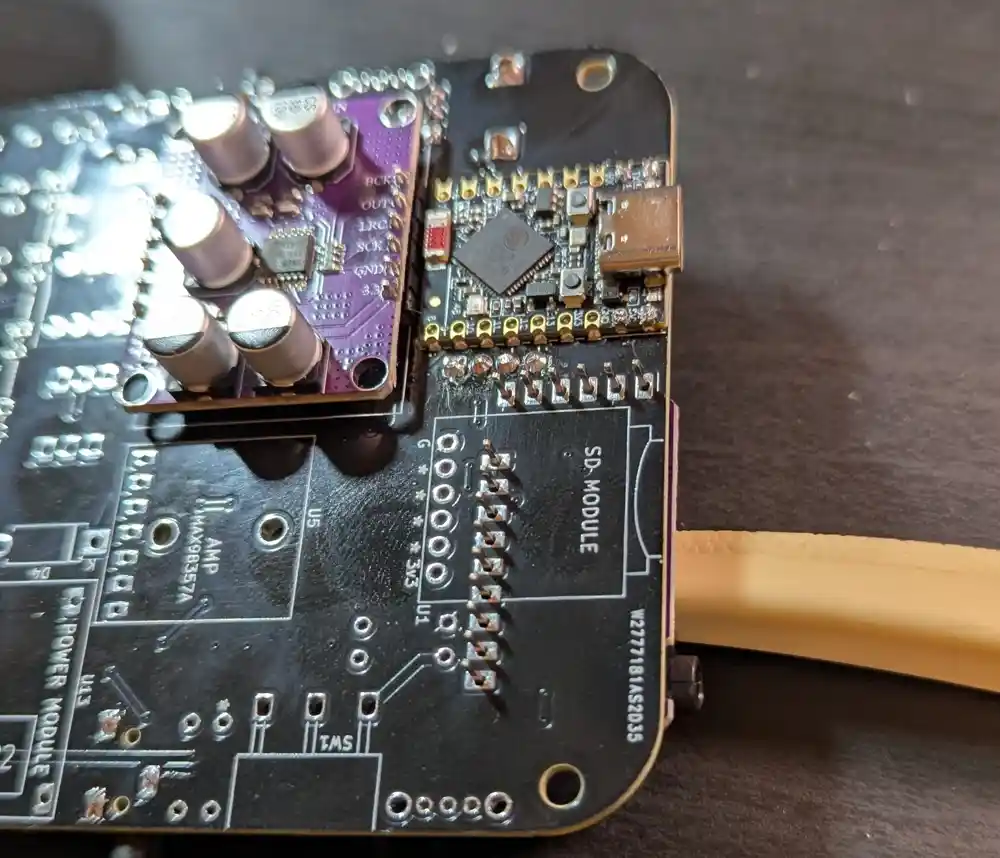
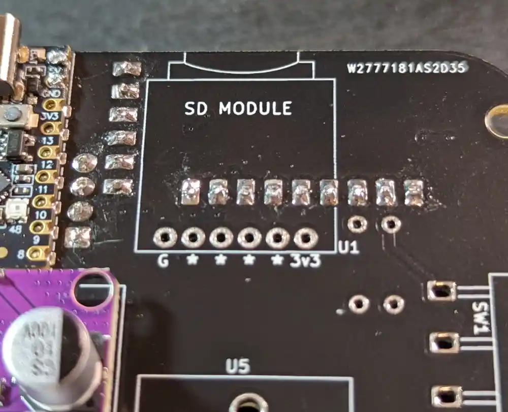
7. SD Module
7.1 SD Module
Next, we’ll be adding the SD module (labeled as such on the PCB) on the bottom of the board.
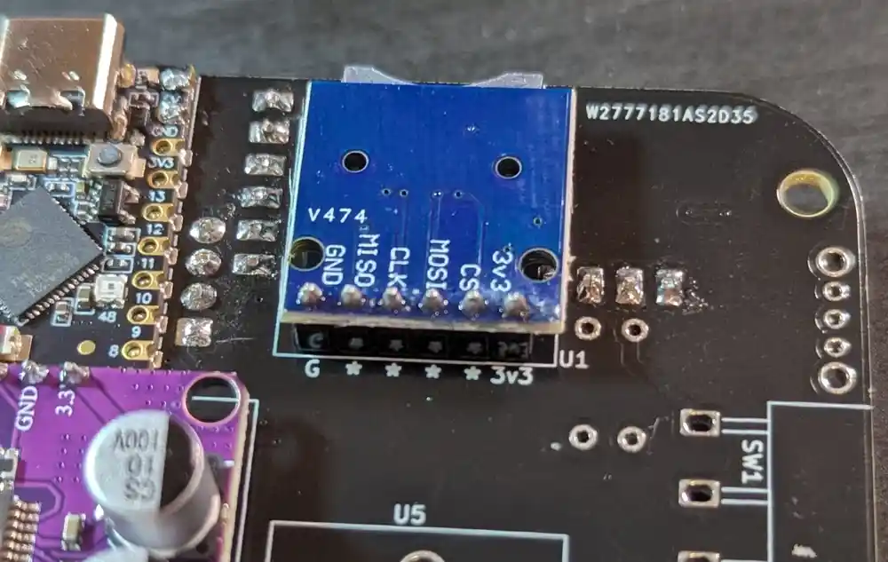
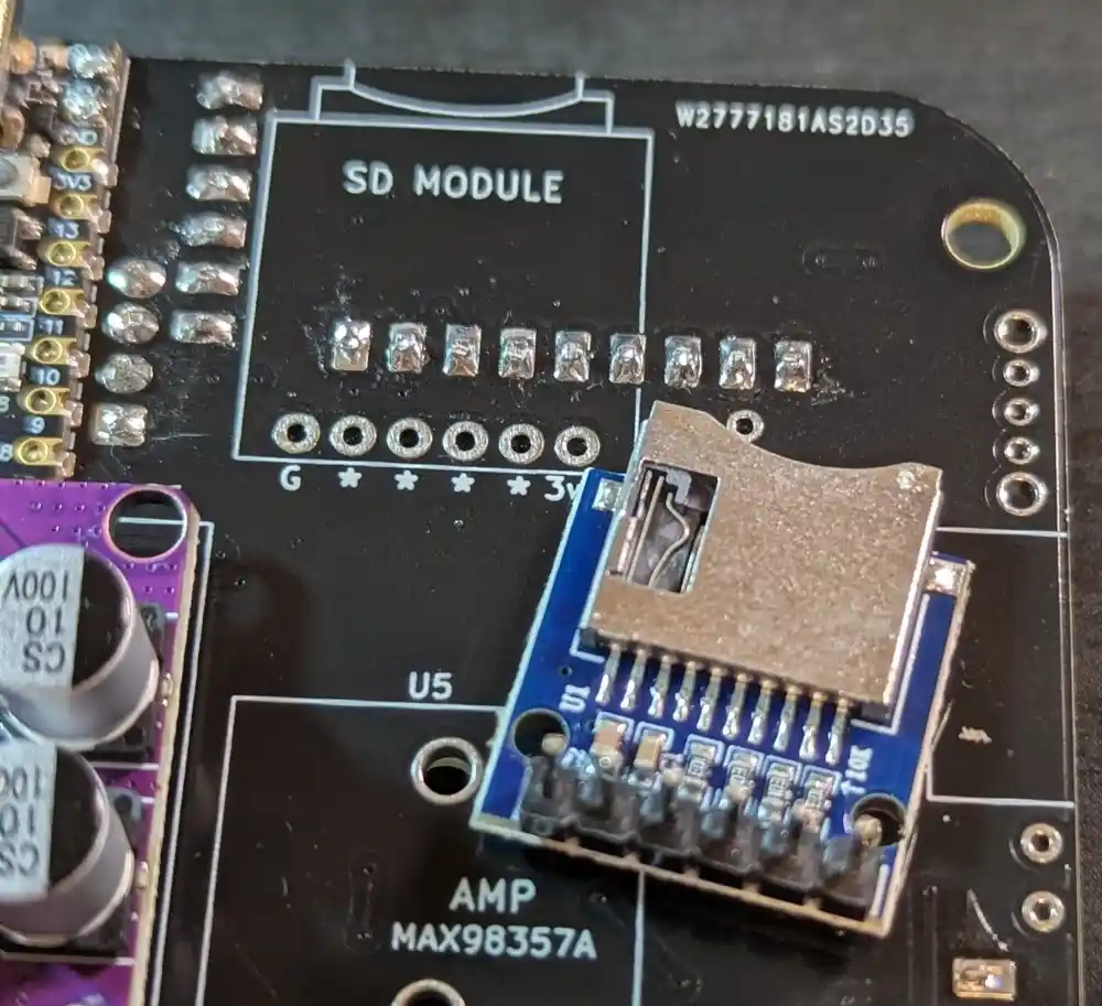
7.2 SD Module (Cont.)
We insert it so that the metal SD slot is sandwiched between the main PCB and the SD module’s PCB.
7.3 SD Module (Cont.)
Next, we can flip the board and solder the module, taking care not to accidentally melt any of the neopixels. We don’t need to snip the legs here.
When the headers are soldered flush to the main PCB, the metal SD slot will stand off the main PCB a little.
8. MAX98357A Module
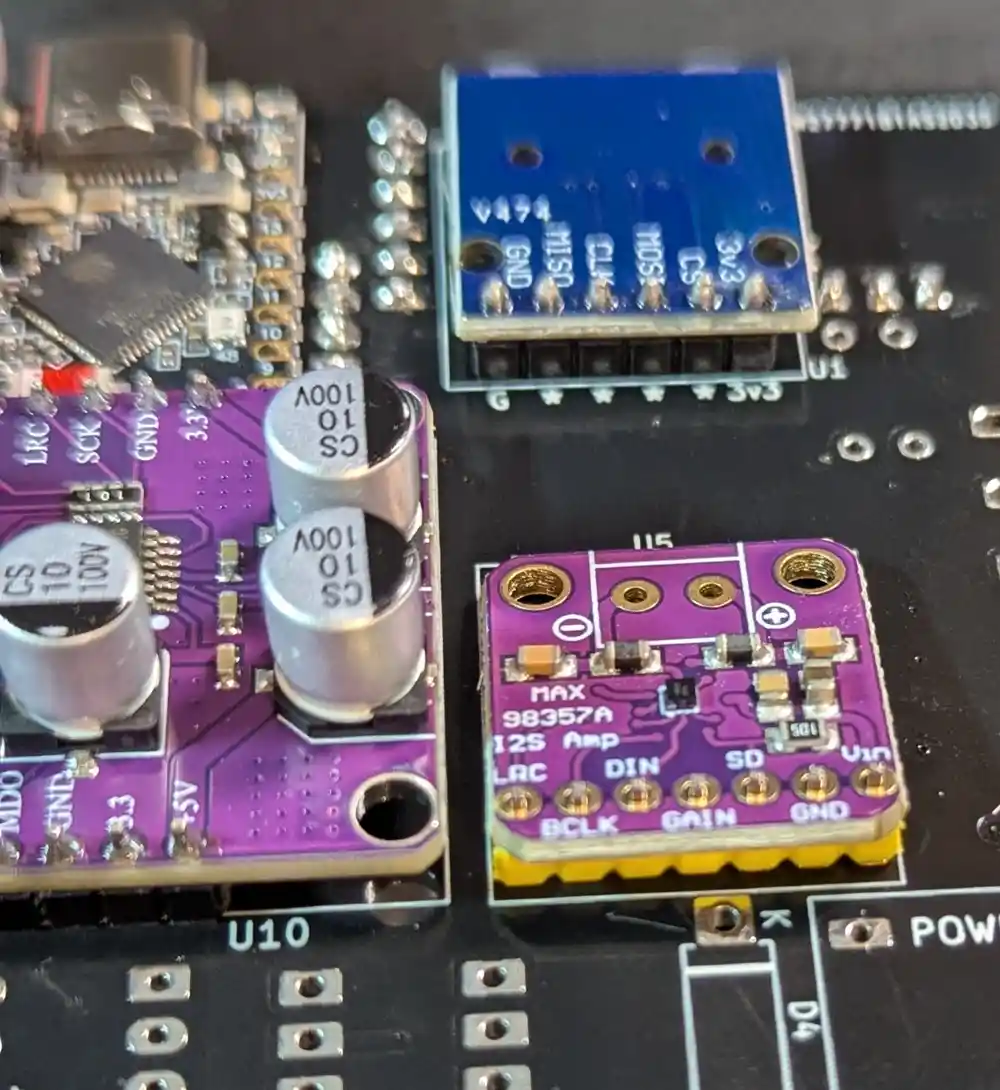
8.1 MAX98357A
On the bottom of the board, we next add the MAX98357A amplifier module, then flip the board and solder the pins. Like the PCM5102, this converts digital I2S audio signals into analog signals to drive our built-in speaker.
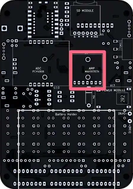
Look for the label AMP MAX98357A.
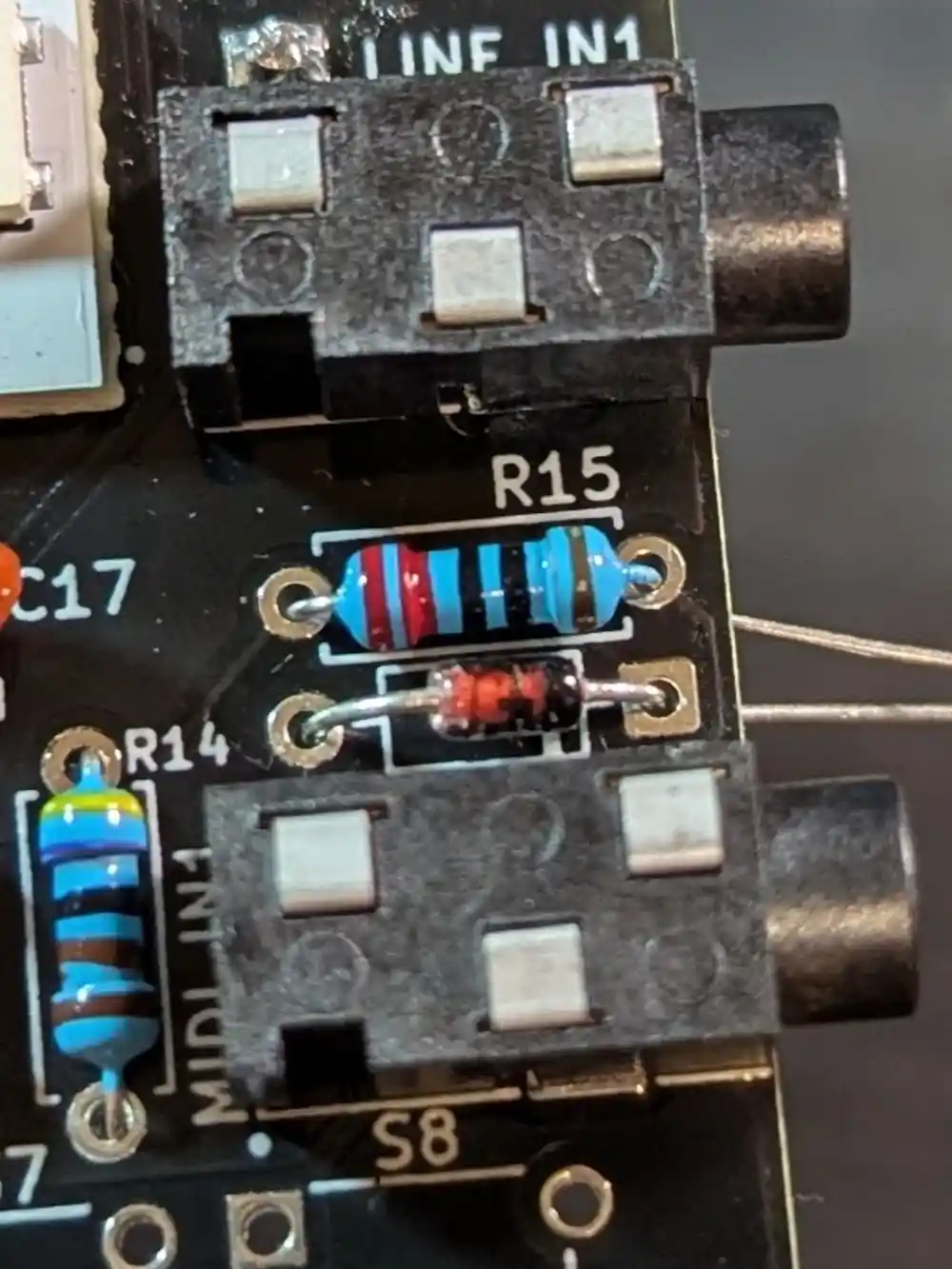
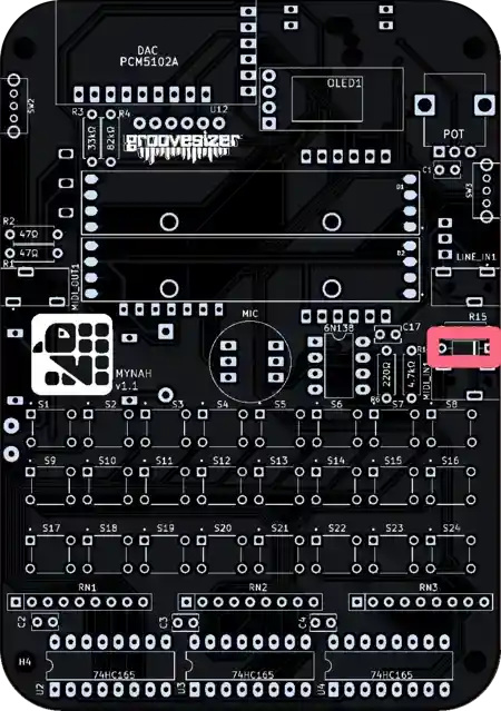
9. Resistors
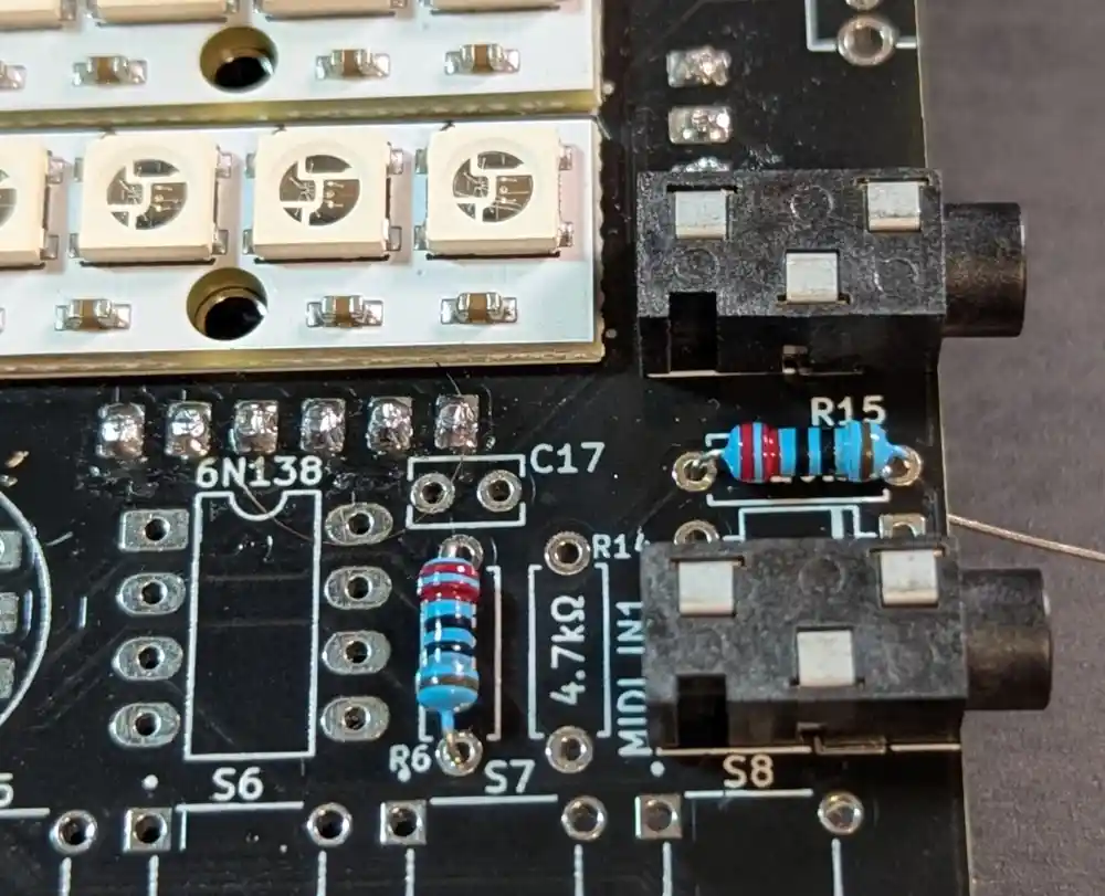
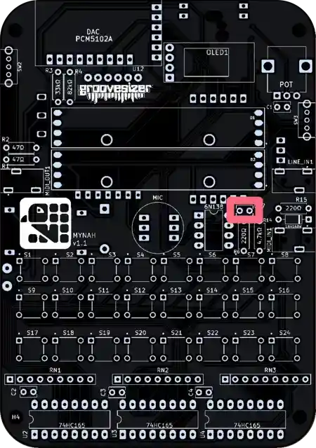
9.1 Resistors (220Ω x2)
Let’s add all the resistors in one go before soldering them all. On the top of the board, we populate the two 220Ω resistors required by our MIDI input circuit – their 5-band color code is Red-Red-Black-Black-Brown and they’re marked R15 and R6 on the PCB. The resistors are all non-polarized and can go in either way around.
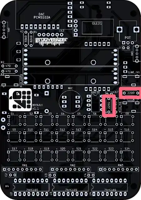
Bend the legs of the resistors to form a U shape before inserting them in the board. They’re labeled R6 and R15 on the PCB.
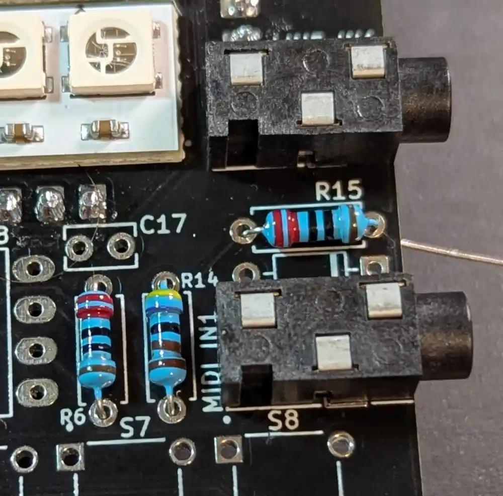
9.2 Resistors (4.7kΩ)
We also populate the 4.7kΩ resistor required for MIDI-in – the 5-band color code is Yellow-Violet-Black-Brown-Brown.
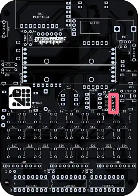
It’s labeled R14 on the PCB.
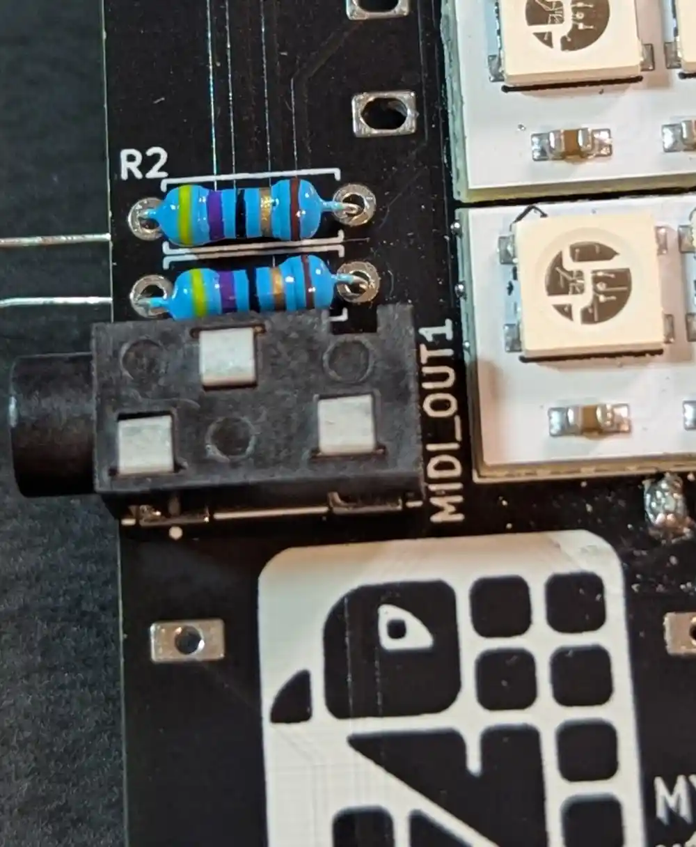
9.3 Resistors (47Ω x2)
Next we populate the two 47Ω resistor required for MIDI-output – the 5-band color code is Yellow-Violet-Black-Gold-Brown.
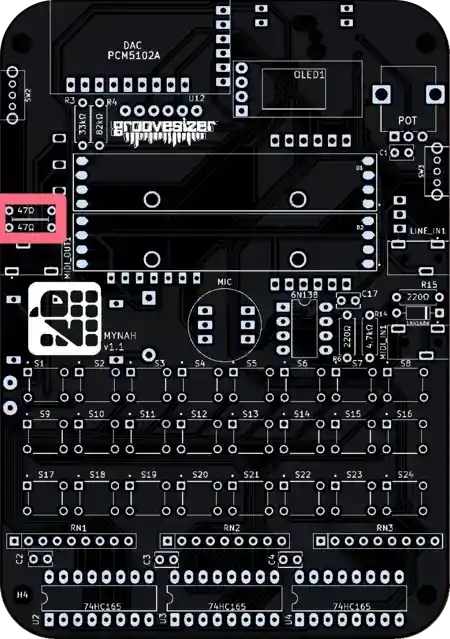
They’re labeled R1 and R2.
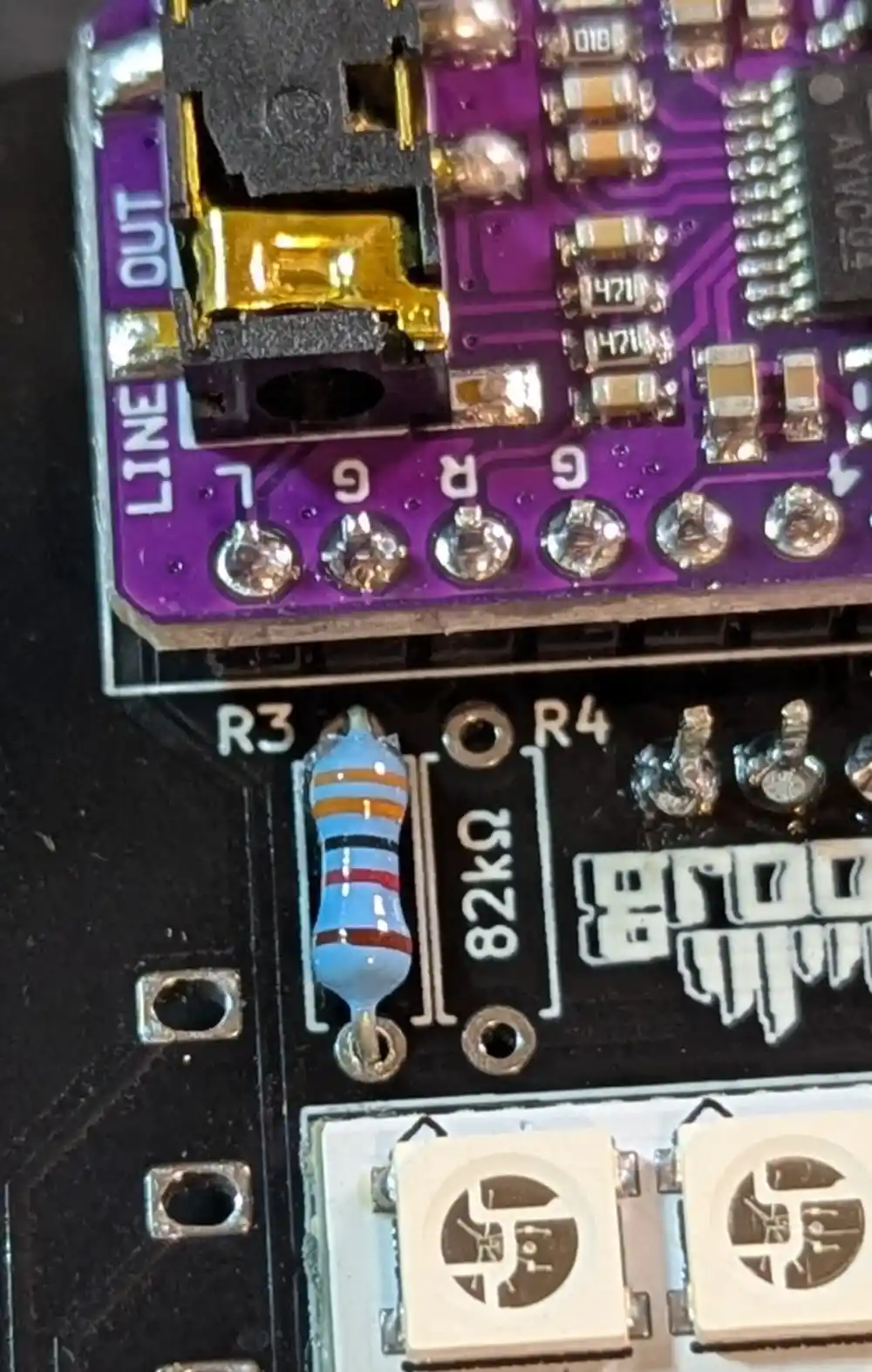
9.4 Resistors (33kΩ)
Then we populate the 33kΩ resistor – the 5-band color code is Orange-Orange-Black-Red-Brown.
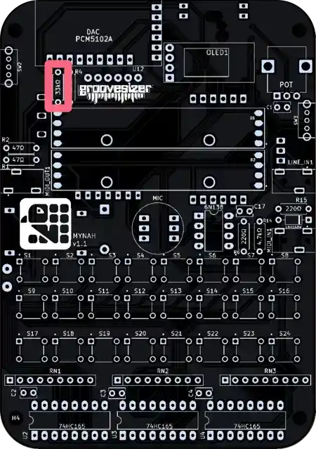
It’s labeled R3.
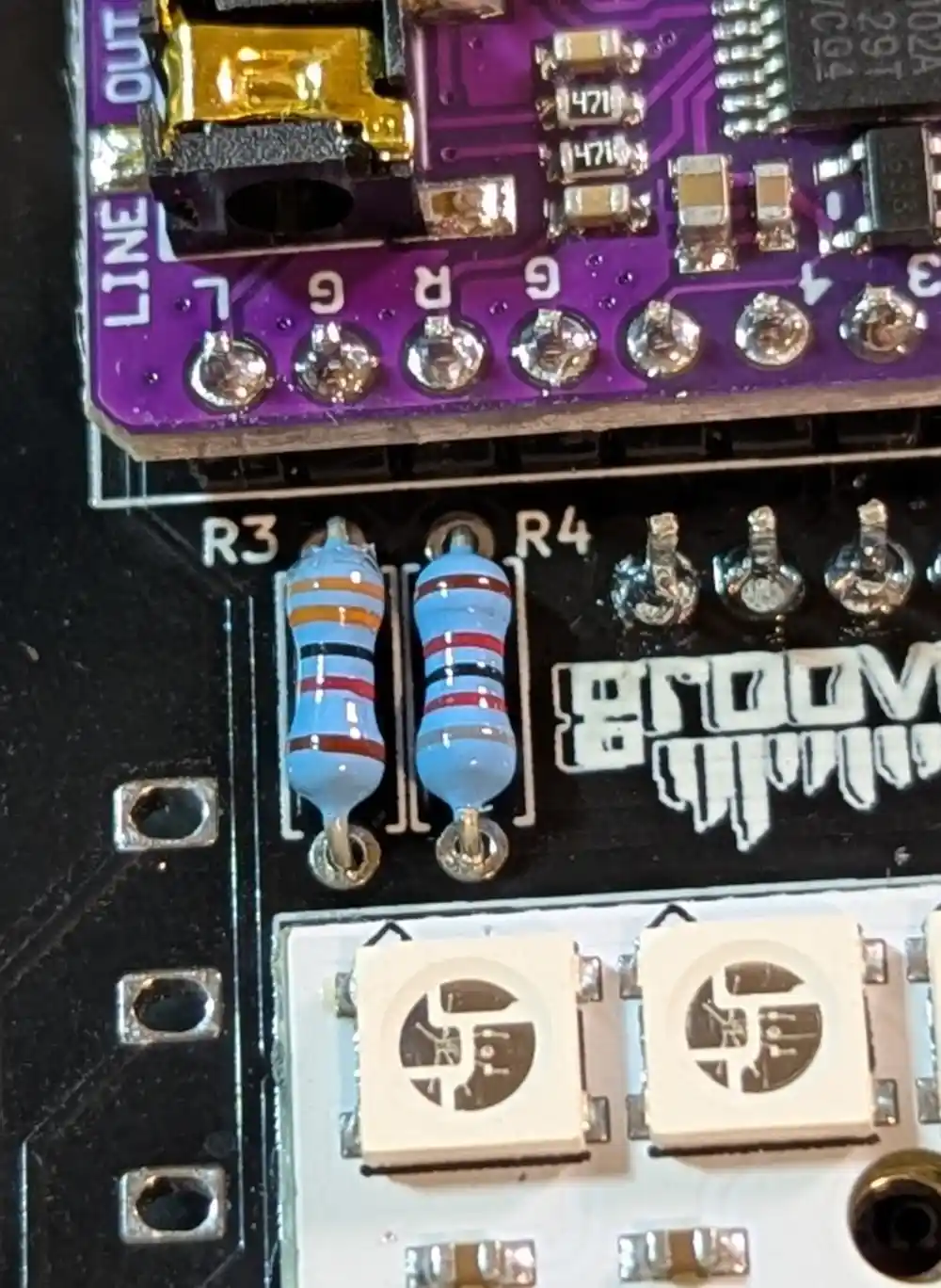
9.5 Resistors (82kΩ)
Finally we add the 82kΩ resistor next to it (labeled R4)- the 5-band color code is Grey-Red-Black-Red-Brown.
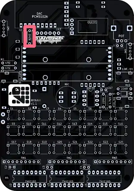
Together, the 33kΩ and 82kΩ resisters form a voltage divider that allows us to measure our battery power (potentially up to 4.5v) safely on a GPIO pin that’s only 3.3v tolerant .
10. Capacitors (100nF)
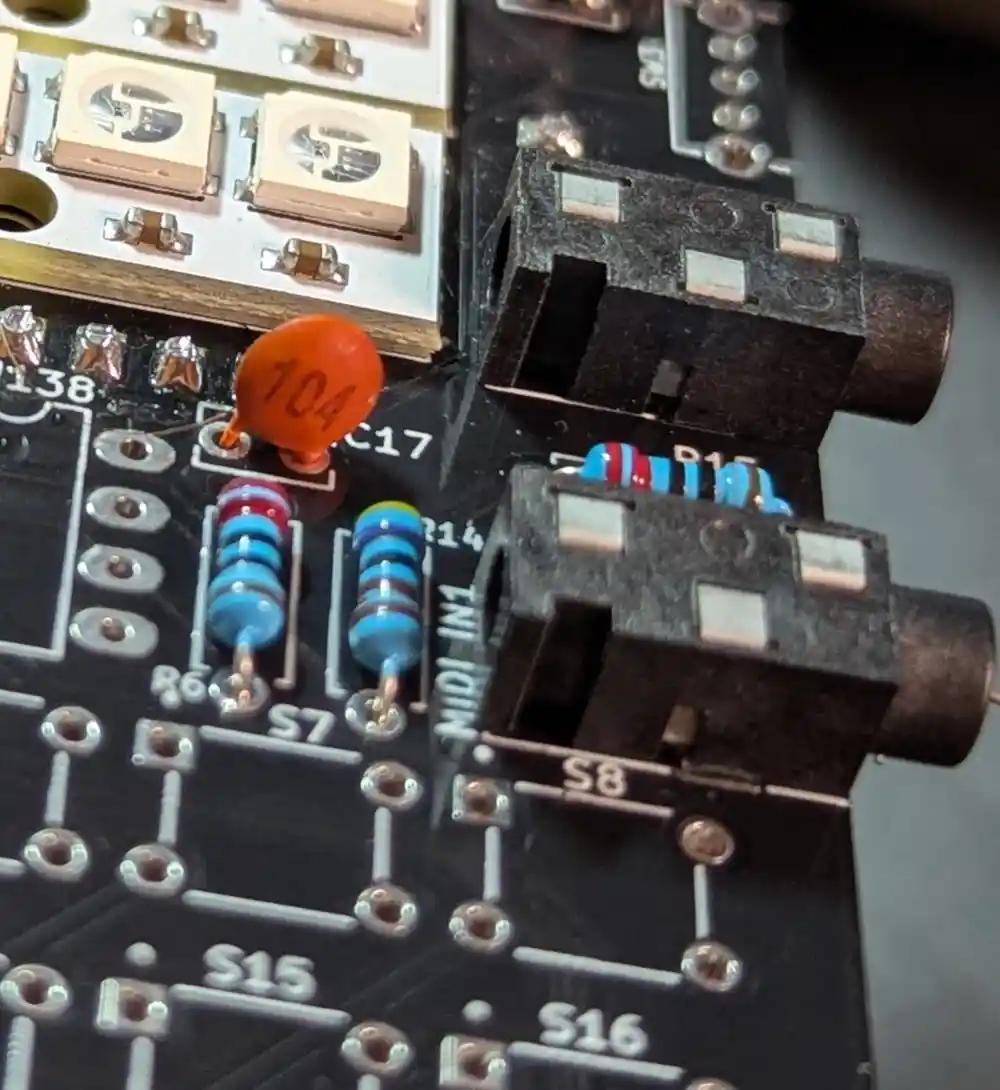
10.1 Capacitors (100nF)
Before we solder, let’s also add the 100nF cap for the MIDI input circuit (it’s marked 104) – either way around is fine
It’s labeled C17.
10.2 Capacitors (100nF x3)
And let’s also add the 3 100nF caps that serve as decoupling caps for the 74HC165 ICs.
They’re labeled C2, C3, and C4.
11. Diode (1N4148)
11.1 Diode (1N4148)
Before we solder, we can also add the 1N4148 for the MIDI input circuit. Watch the orientation – the black line on the diode body should match the white line on the footprint.
On the PCB, it’s labeled 1N4148W in microscopic text.
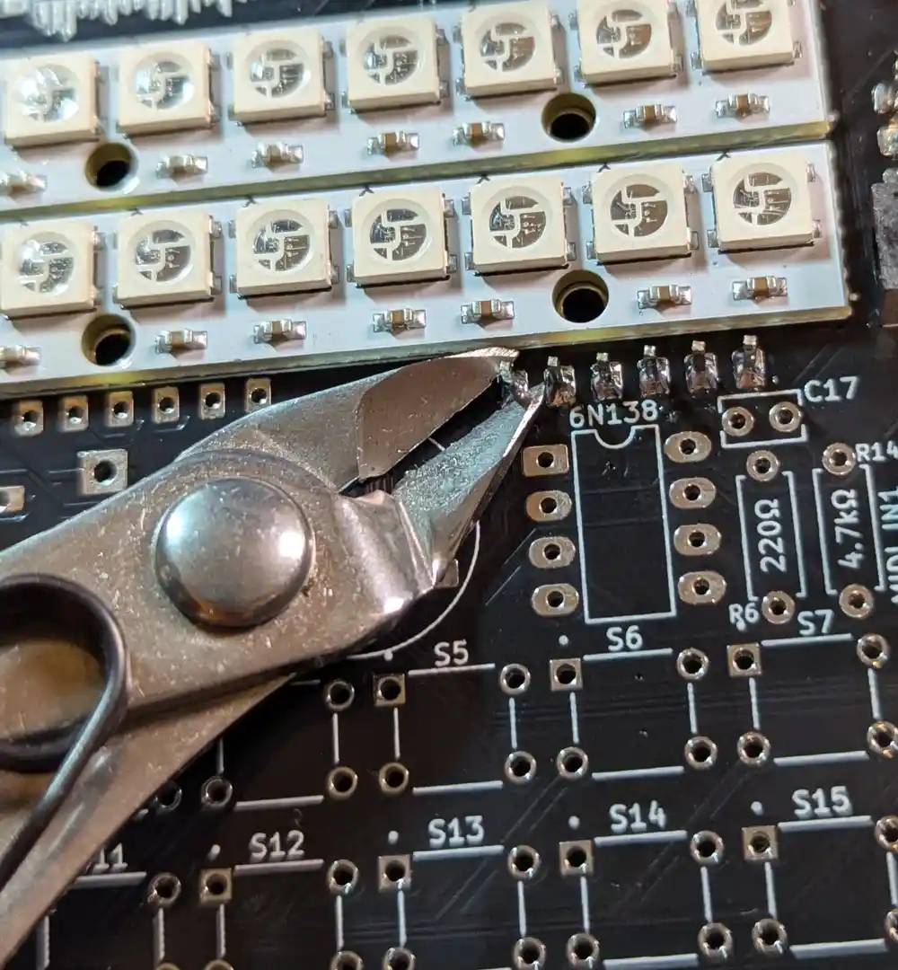
11.2 Diode (1N4148 – Cont.)
Now we can flip the board, then solder and snip all the legs for the components we just added.
12. Diode (SB240)
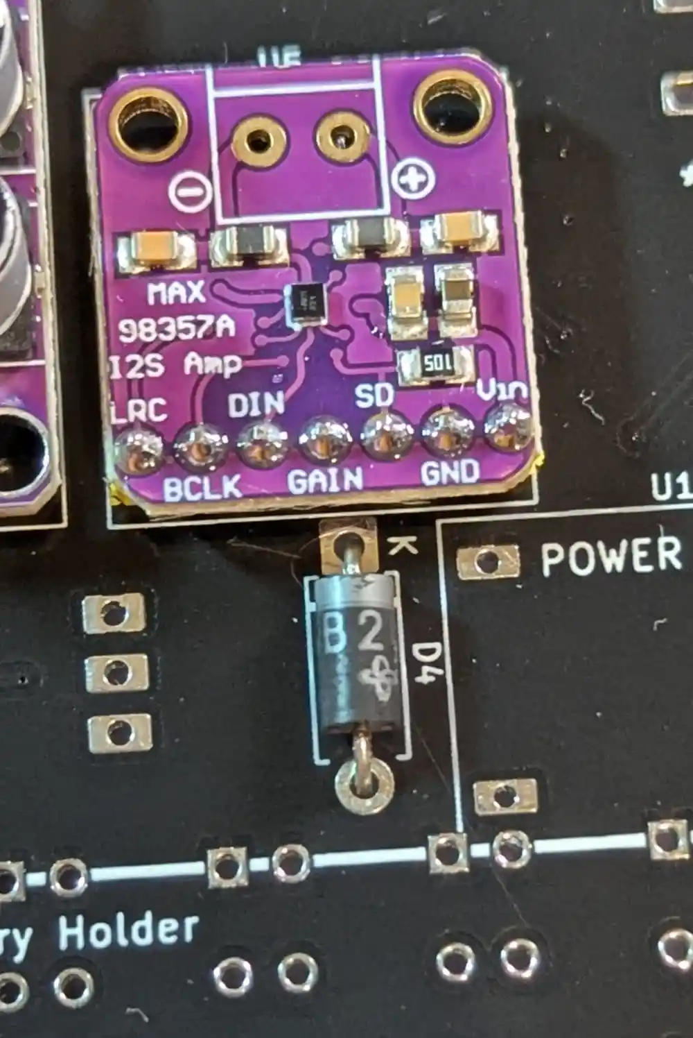
12.1 Diode (SB240)
On the bottom of the board, we can now add the larger diode. The orientation is important here too. The silver side of the diode body aligns with the line on the footprint.
It’s marked as D4. The diode prevents the USB power rail from back-feeding current into the battery pack when both power sources are connected simultaneously.
13. Optocoupler IC (6N138)
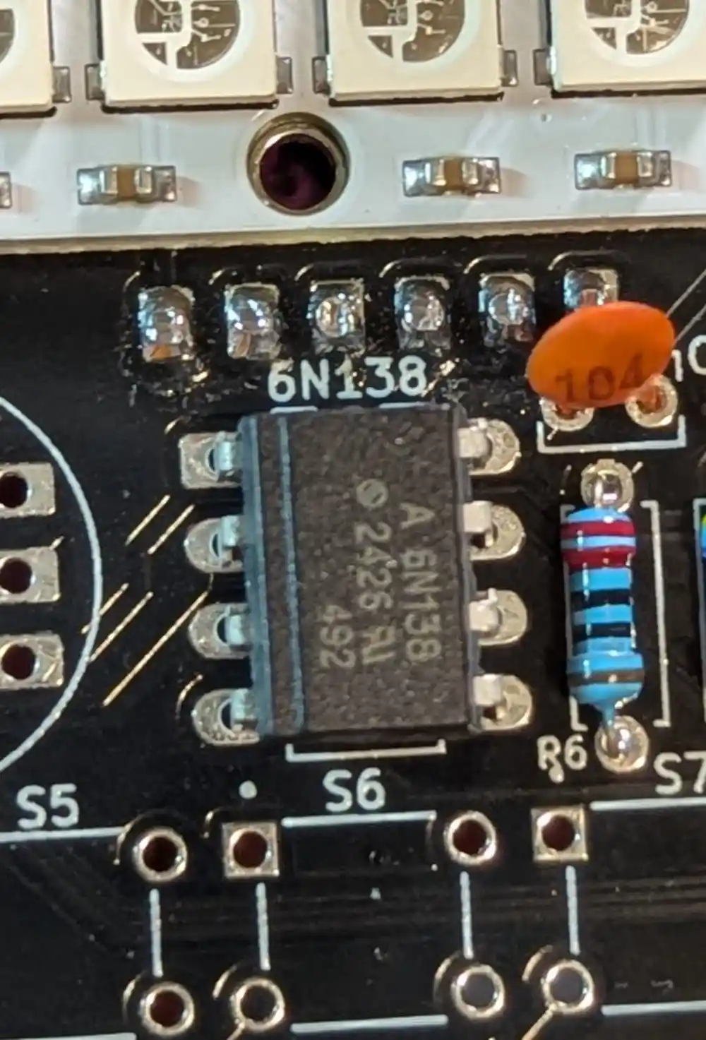
13.1 Optocoupler IC (6N138)
The footprint is marked 6N138 on the top of the board. Be careful with the orientation – pin 1 is top left with the square pad. In this case, the beveled edge should be on the left. After triple checking the orientation, flip and solder.
The 6N138 physically separates the input and output electrical paths in our MIDI input circuit.
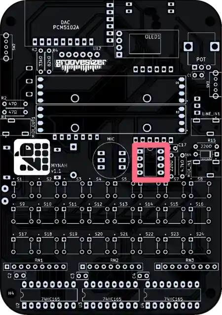
14. Microphone (INMP441)
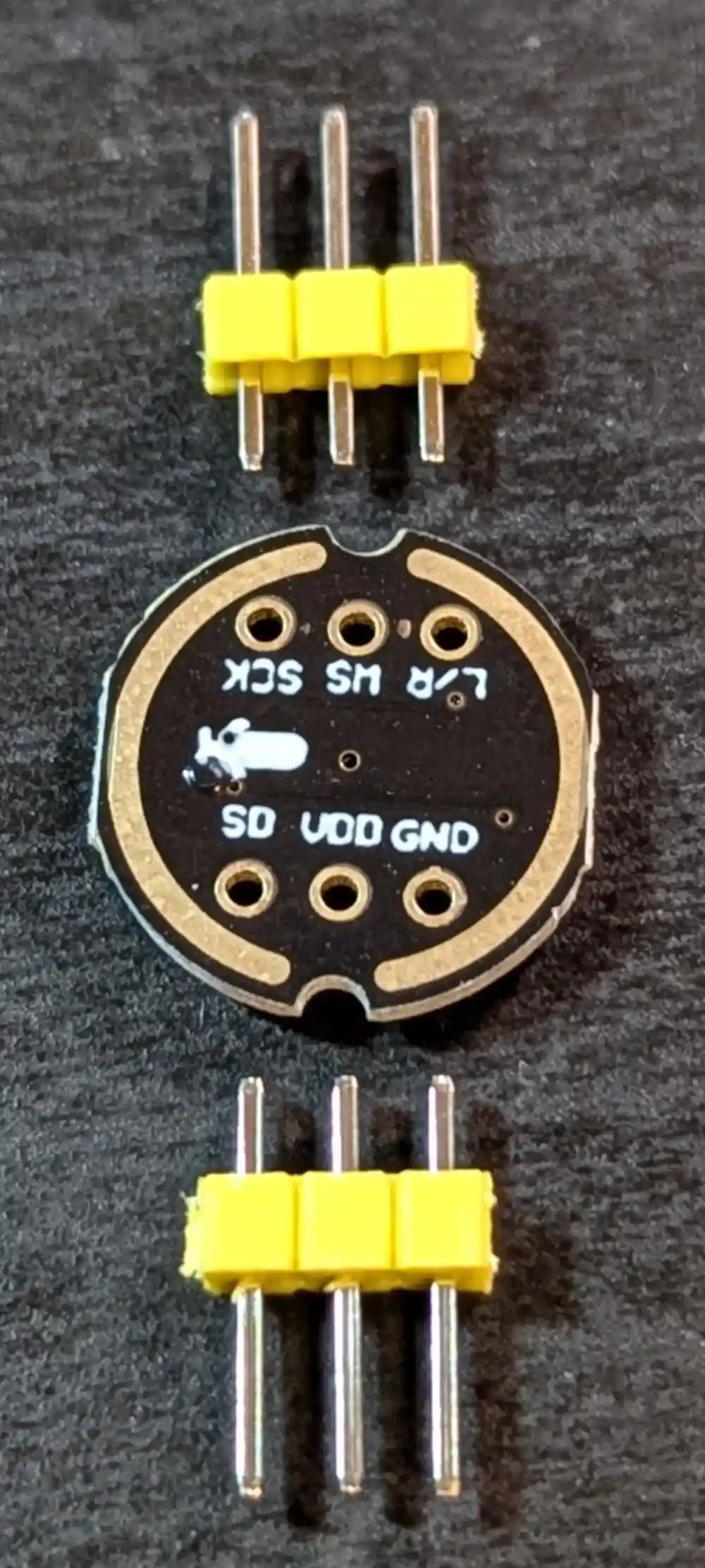
14.1 Microphone (INMP441)
The headers have been cut to size, so we can just insert them in the PCB
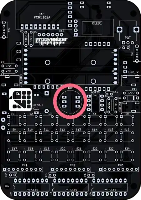
Also located on the top of the board, the footprint is marked MIC.
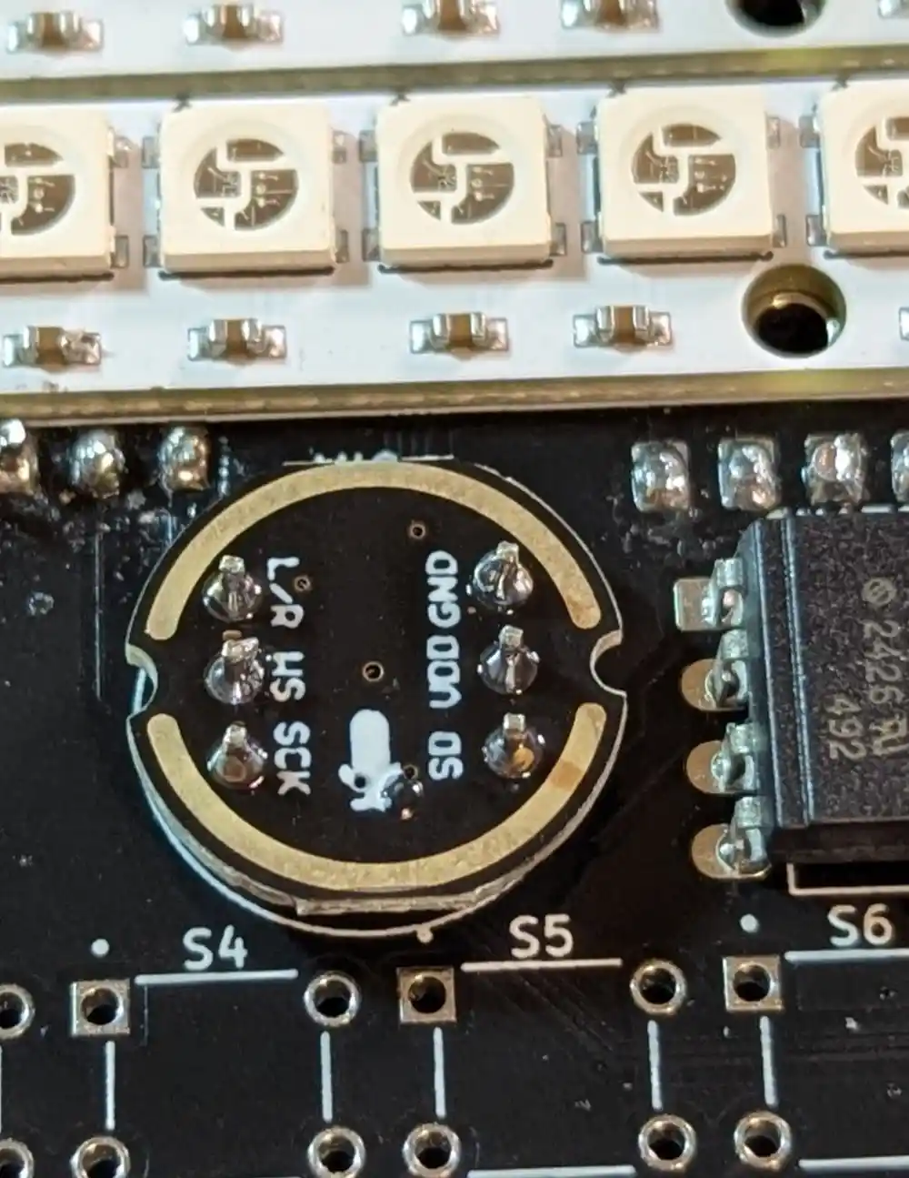
14.2 Microphone (INMP441 – Cont.)
Orientation is important here, too. The GND pin is located top right. Do ensure the the MIC module is flush with the headers and the headers are flush with the PCB when soldering.
The INMP441 MEMS mic has a built-in analog-to-digital converter (ADC) and outputs data via the I2S interface allowing direct connection to the ESP32.
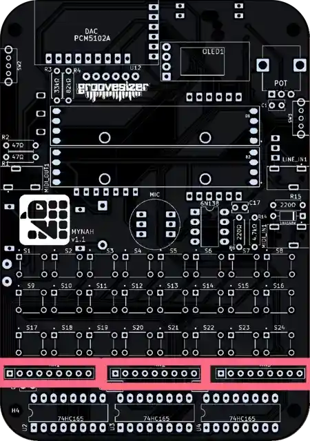
15. Shift Register ICs (74HC165)
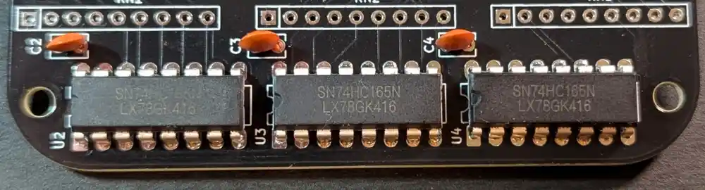
15.1 Shift Register ICs (74HC165) x3
The 3 shift register ICs allows us to read all 24 button inputs with only 3 pins on the ESP32. The orientation is important. The notch in the casing should be on the left. Flip and solder.
Located on the top side of the board, the footprints are labeled U2, U3 and U4.
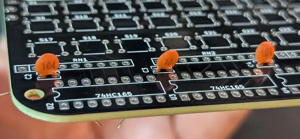
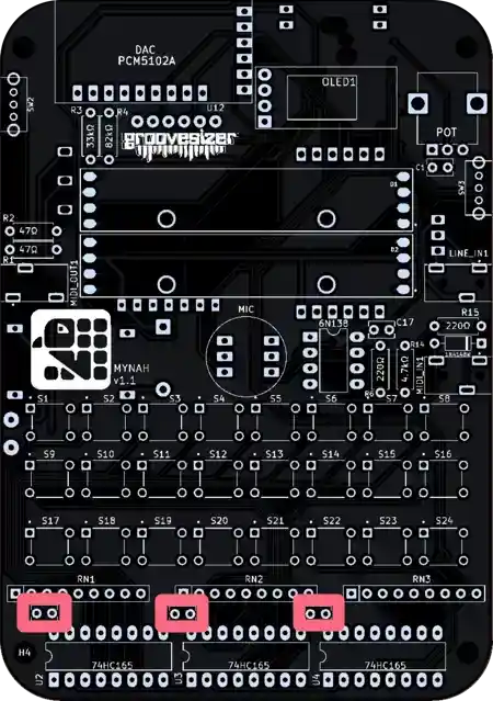
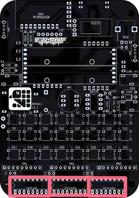
16. Resistor Networks (10kΩ)
16.1 Resistor Networks (10kΩ) x3
Let’s add and solder the 3 resistor networks required by the shift register ICs.
The footprints are labeled RN1, RN2 and RN3. The common pin is marked on the PCB with a square pad. There’s a dot printed on the resistor network to indicate the common pin side.
17. Small Slide Switches
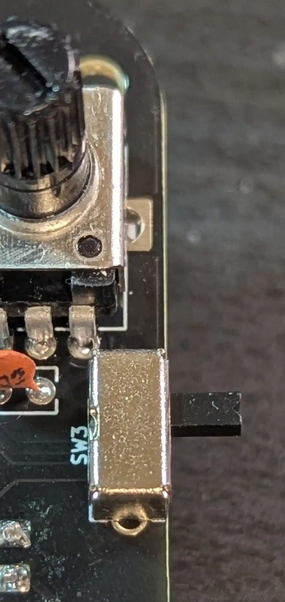
17.1 Small Slide Switches x2
On the top side of the board, the small slide switches are marked as SW2 and SW3
The switch on the right selects between MIC and LINE inputs.
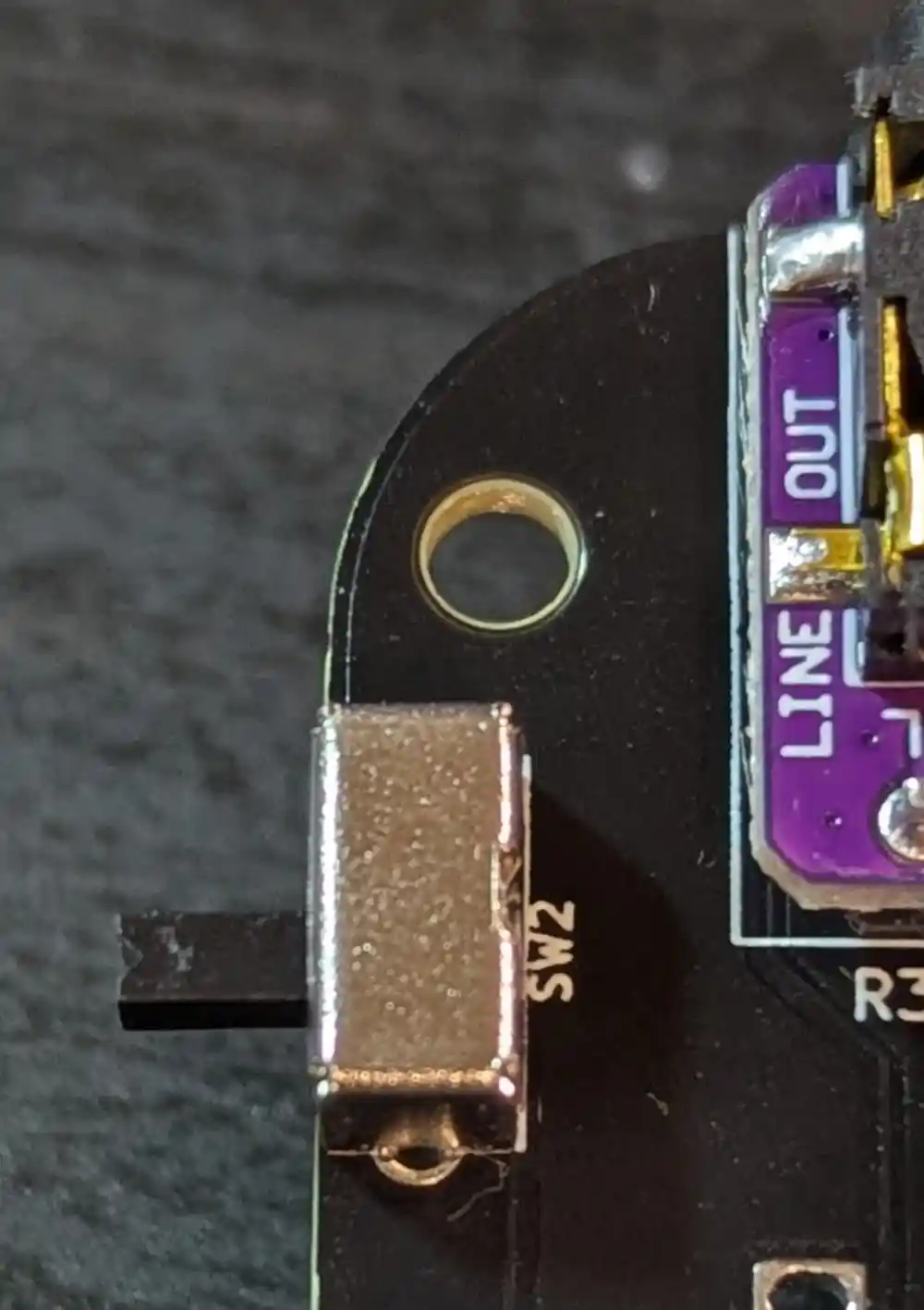
17.2 Small Slide Switches x2 (Cont.)
The switch on the left turns our built-in speaker on and off.
18. Battery Power Switch
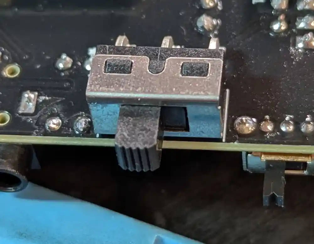
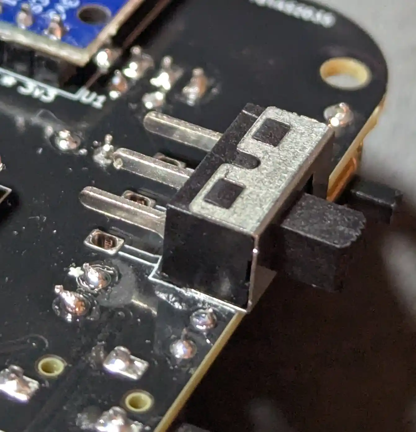
18.1 Battery Power Switch (right-angle)
We need a beefier solution for the battery power switch. It’s good practice to switch off battery power when the Mynah is plugged in via USB C, but the diode we added earlier is intended to prevent damage if you forget.
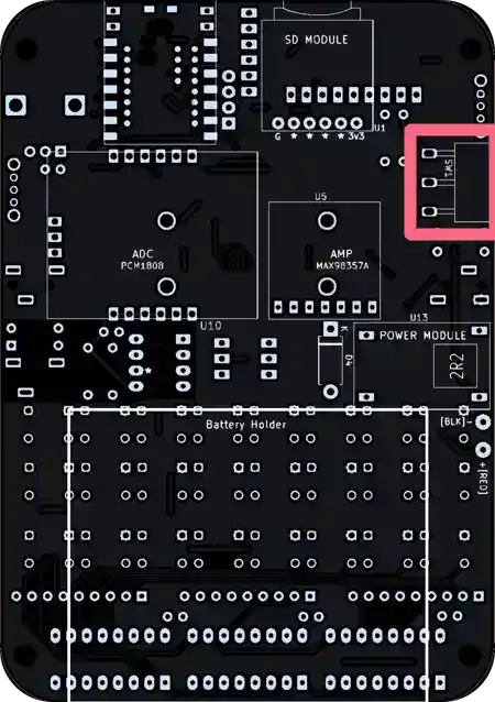
The footprint is located on the bottom of the board and it’s marked SW1.
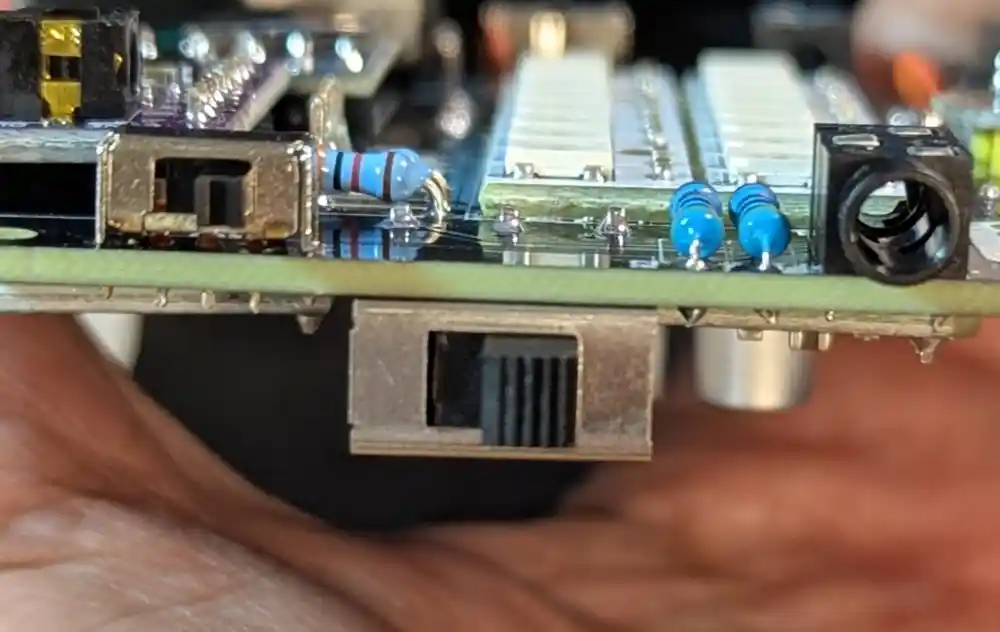
18.2 Battery Power Switch (Cont.)
It will be hard to fit the PCB in the enclosure if the large switch is not flush against the PCB. It should look like the image.
18.3 Battery Power Switch (Straight)
Please note that some kits ship with switches with straight legs in cases where the right-angle version is not available. Admittedly, its a less elegant solution, since it requires glue to affix the switch to the PCB. To glue it down, use two-part epoxy, hot melt glue, or superglue. The switch can be affixed either way around, but make sure that the body does not protrude over the edge of the PCB, or it may not fit in the enclosure properly.
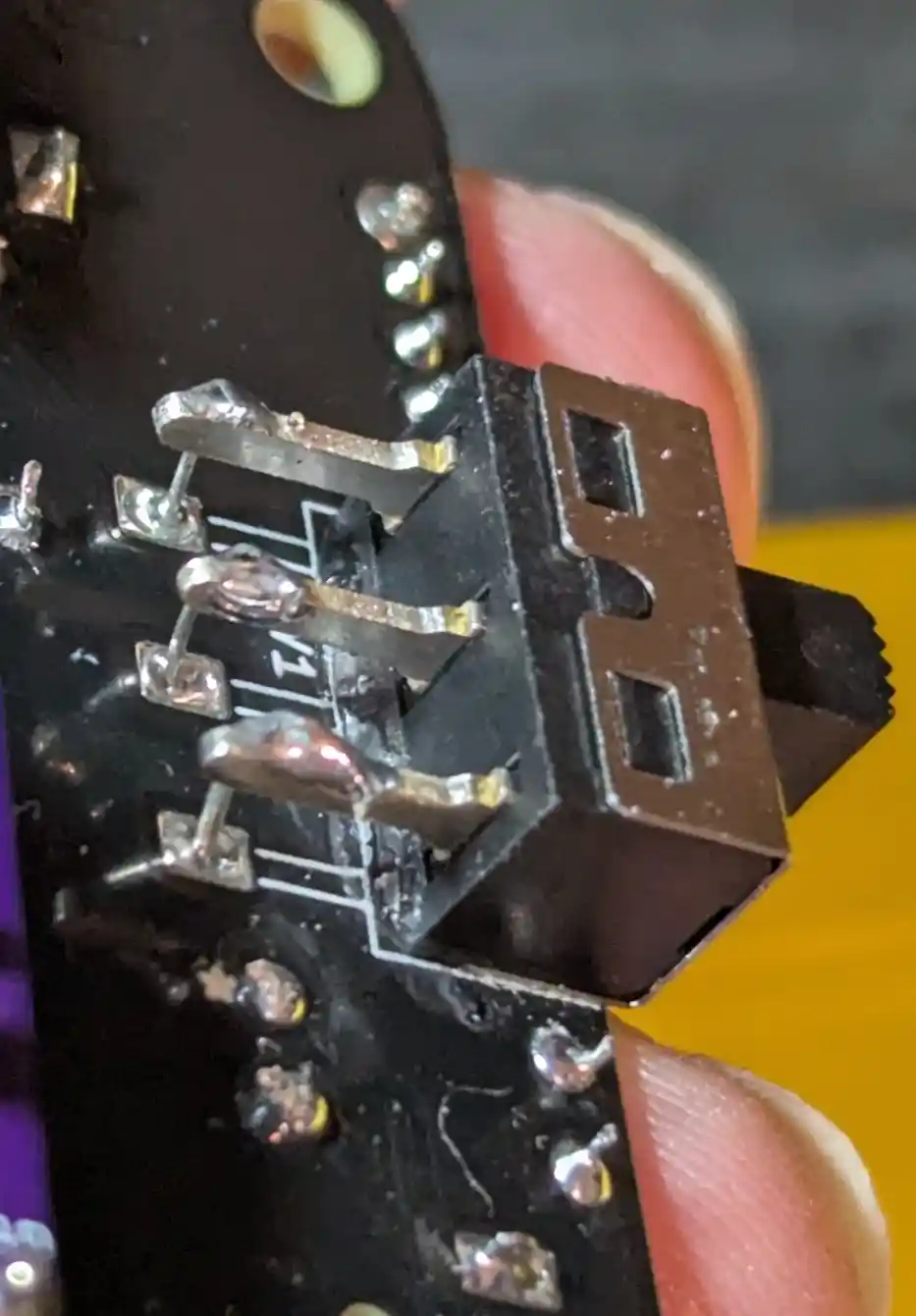
18.4 Battery Power Switch (Straight Cont.)
Grab three of the resistor legs we cut off in step 11.2, give them a walking stick hook at one end, then solder them in to bridge the switch legs to the pads.
19. Tactile Switches
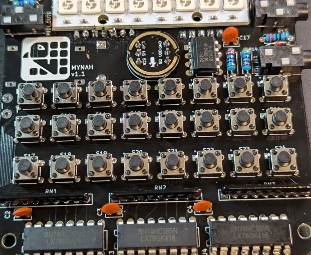
19.1 Tactile Switches x24
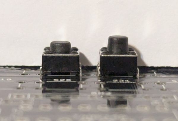
HOLD UP:
A number of kits were shipped with switches with 5mm instead of 6mm stems. While they work electrically, the button caps don’t press-fit correctly and will fall off. If you’re affected, you should have received an email informing you that a replacement set is on the way. In the meantime, please pause at this step until it arrives. Apologies!
Go ahead and insert all 24 tactile switches on the top of the PCB. With the switch oriented with the legs on the sides (not top and bottom), it can go in either way around. It’s very important these guys are straight, so definitely solder one leg of all switches first, confirm the alignment by looking at the rows from the sides, then solder the remaining legs.
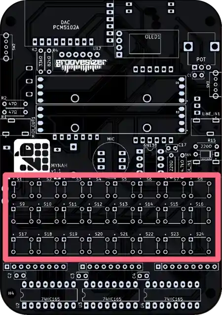
The footprints are marked S1-S24.
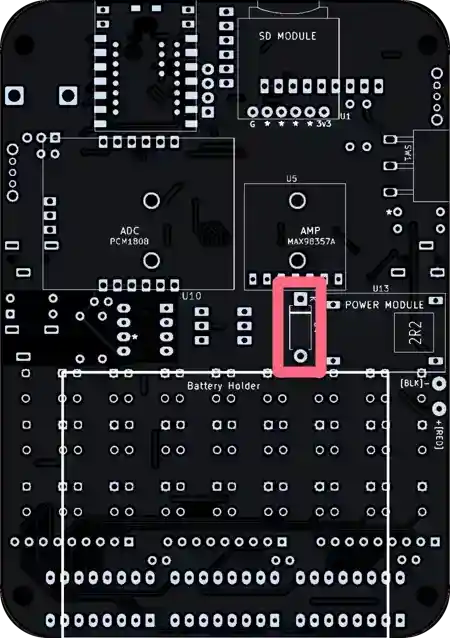
20. Power Module (5V 3A)
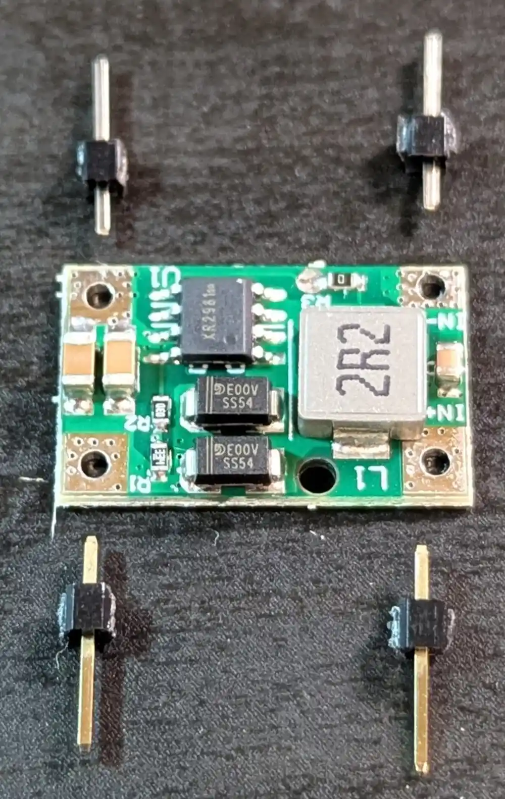
20.1 Power Module (5V 3A)
Phew, almost there! Next we want to add the power module that provides stable 5V from our AA battery pack. We’ll need to separate a 4 pin header into 4 individual pins.
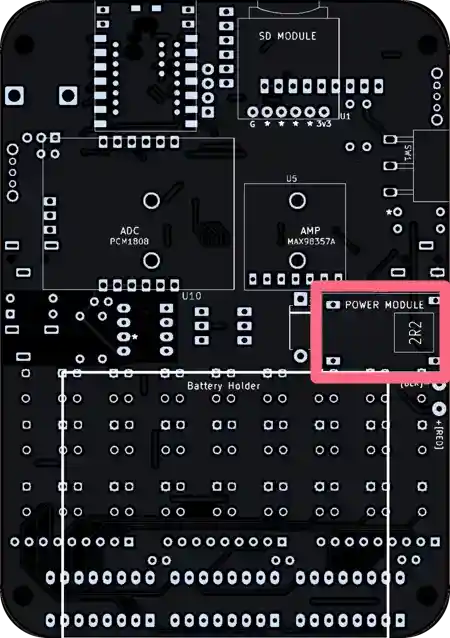
The footprint is located on the bottom of the board and is marked both POWER MODULE and U13.
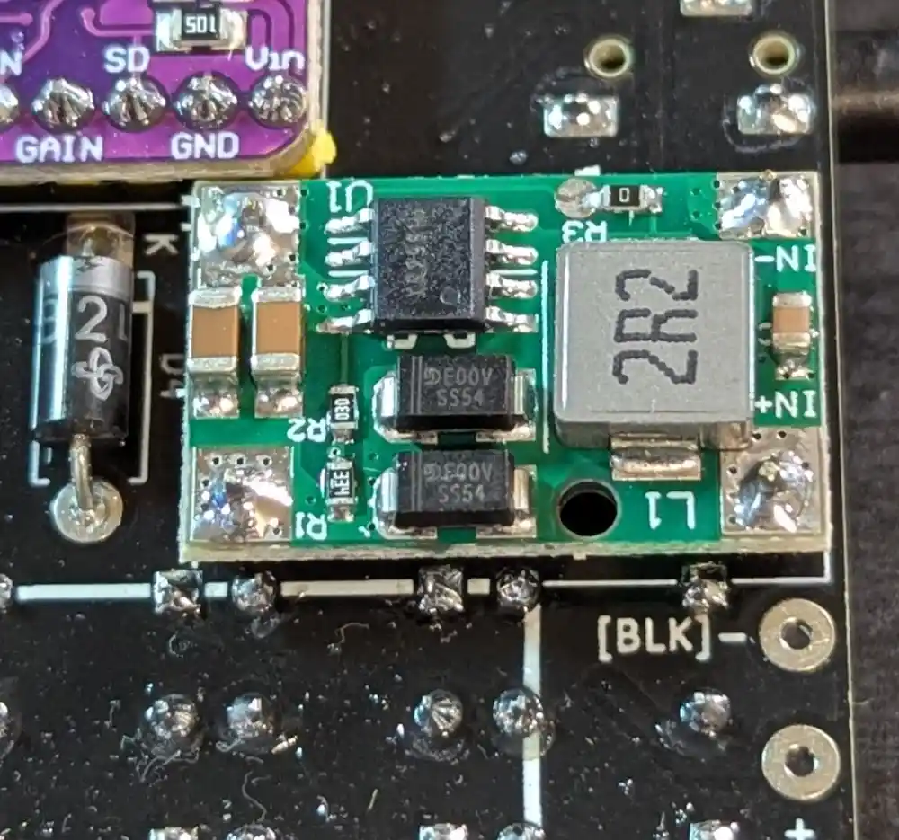
Make sure the orientation matches the footprint with the large 2R2 component on the right side.
21. Battery Holder
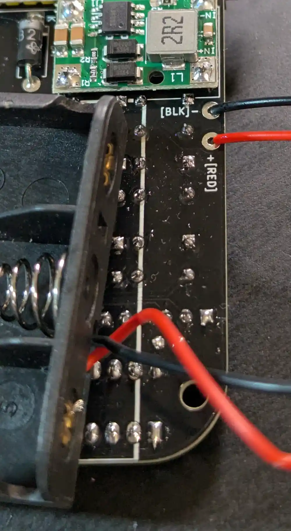
21.1 Battery Holder
On the bottom of the PCB. let’s solder the battery holder leads to the PCB.
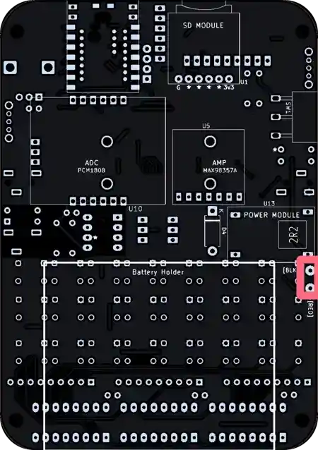
The red and black wires have pads marked as such.
22. Speaker (8Ω)
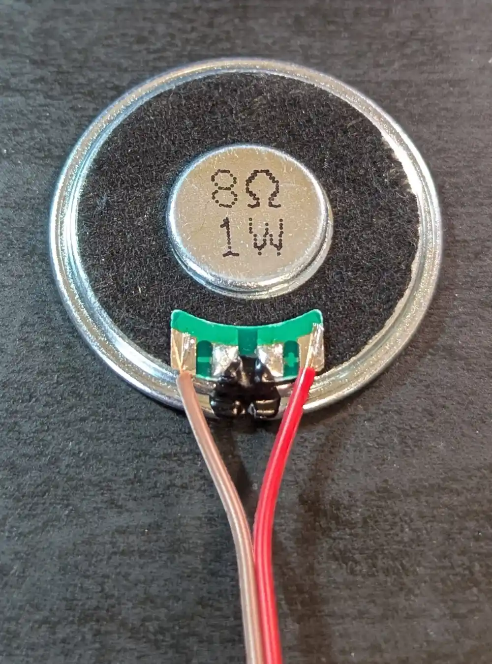
22.1 Speaker (8Ω)
Aha, there’s no footprint for the speaker leads, because it’s soldered to the amp module.
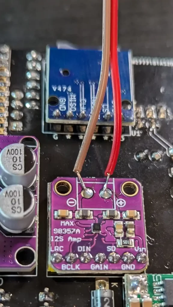
The red lead goes to positive (+) on the amp PCB, and black or brown goes to negative (-).
23. Enclosure
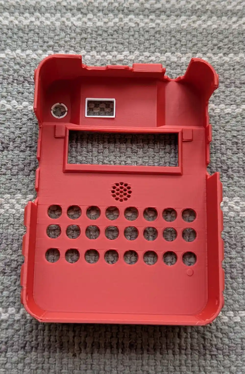
23.1 Enclosure
You will receive the enclosure with all the M3 screws in place (8 black ones and one thumb screw). Undo the 4 screws on the sides of the enclosure and remove the top.
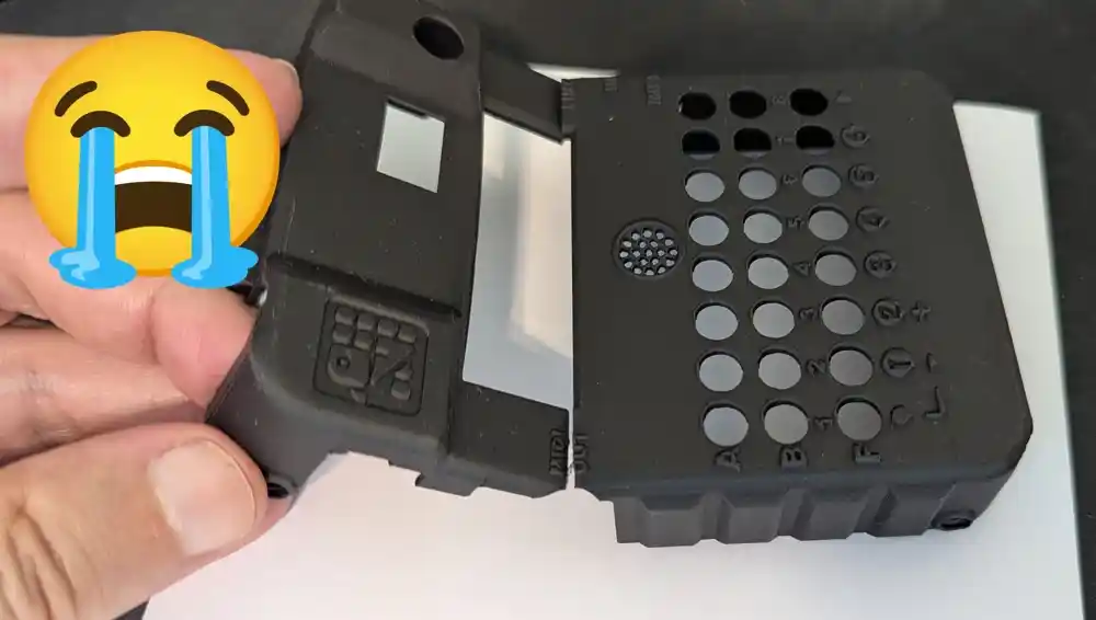
CAUTION: Be careful not to bend the enclosure top when removing it from the bottom, and don’t apply pressure from the sides when the top is not screwed on the bottom. While it’s perfectly robust when everything is screwed in place, the enclosure lacks structural strength when taken apart and can easily crack, especially around the large opening for the neopixel sticks.
23.2 Enclosure (Cont.)
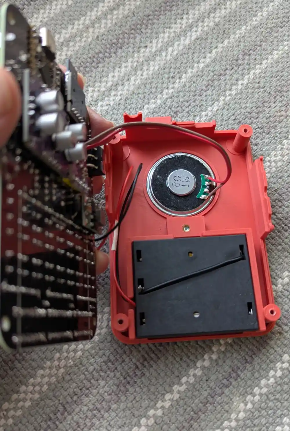
Drop the speaker face-down into its hole in the enclosure bottom. I would advise against gluing it in, since the lead is soldered to the PCB. Instead you can use small strips of double sided tape to keep it in place – tiny beads of Prestik (reusable putty) work fine too.
Also insert the battery holder face down into its space. The leads should be on the left side and exit through the slot.
23.3 Enclosure (Cont.)
Remove the 4 corner screws from the standoffs of the enclosure bottom, then place the PCB on the standoffs, making sure not to pinch any wires.
You can add the white diffuser over the neopixels now. It’s a friction fit and doesn’t exactly snap in place, but it will be held in place securely when the top is screwed on.
And it’s also time to add the button caps. These are similarly a friction fit – just push them on.
23.4 Enclosure (Cont.)
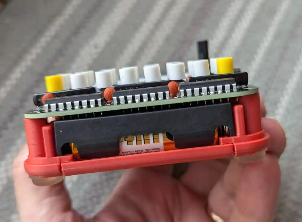
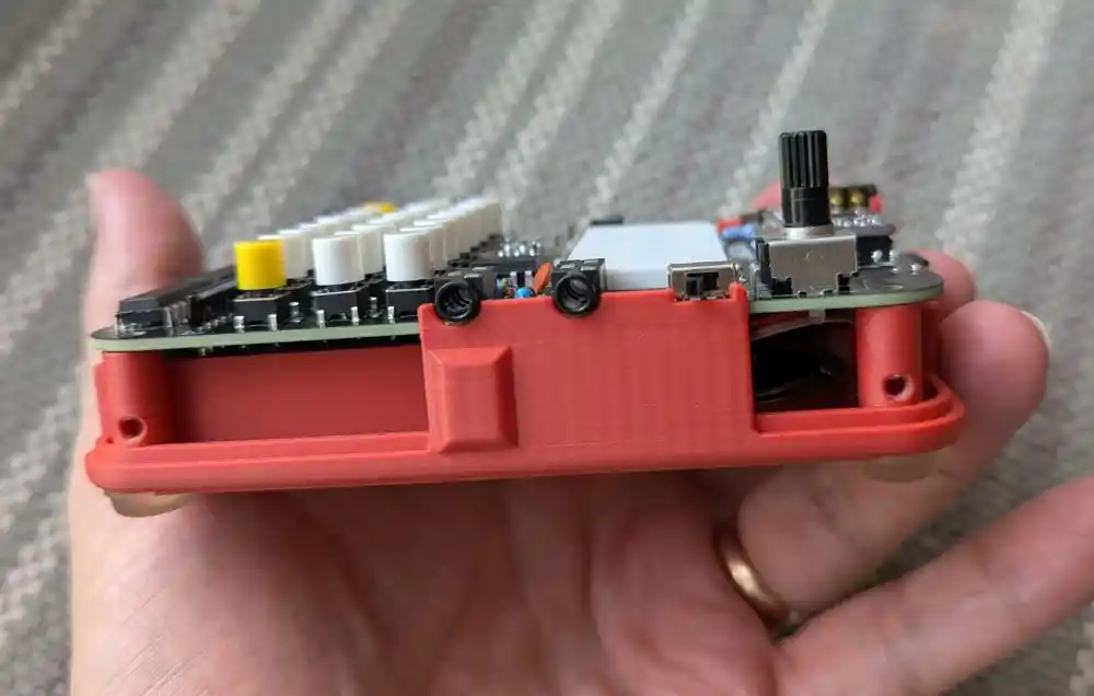
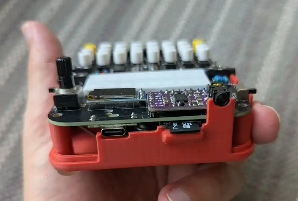
Screw in the 4 corner screws so that the PCB is held tight against the standoffs. However, be careful not to overtighten them as the thread can strip – unlike for the battery compartment thumb screw which has a brass insert, the black enclosure screws screw straight into the plastic. In our extensive testing, this is a perfectly reliable solution as long the screws are not overtightened.
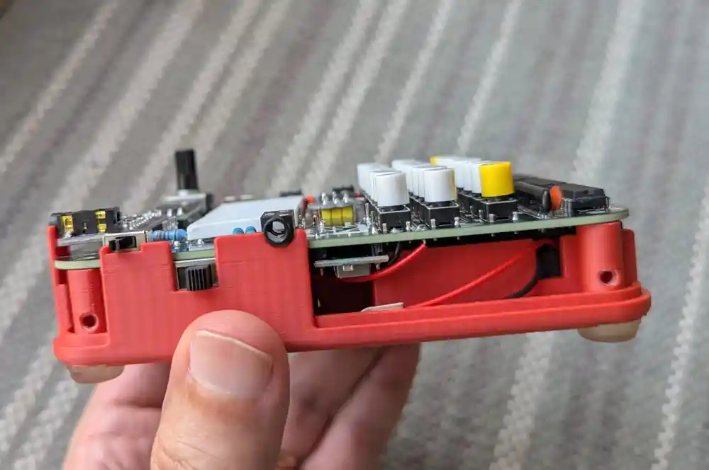
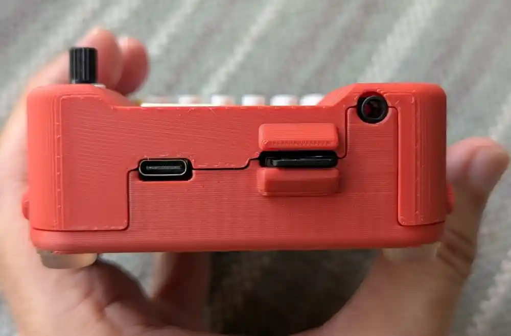
Here’s what we expect to see from the sides.
23.5 Enclosure (Cont.)
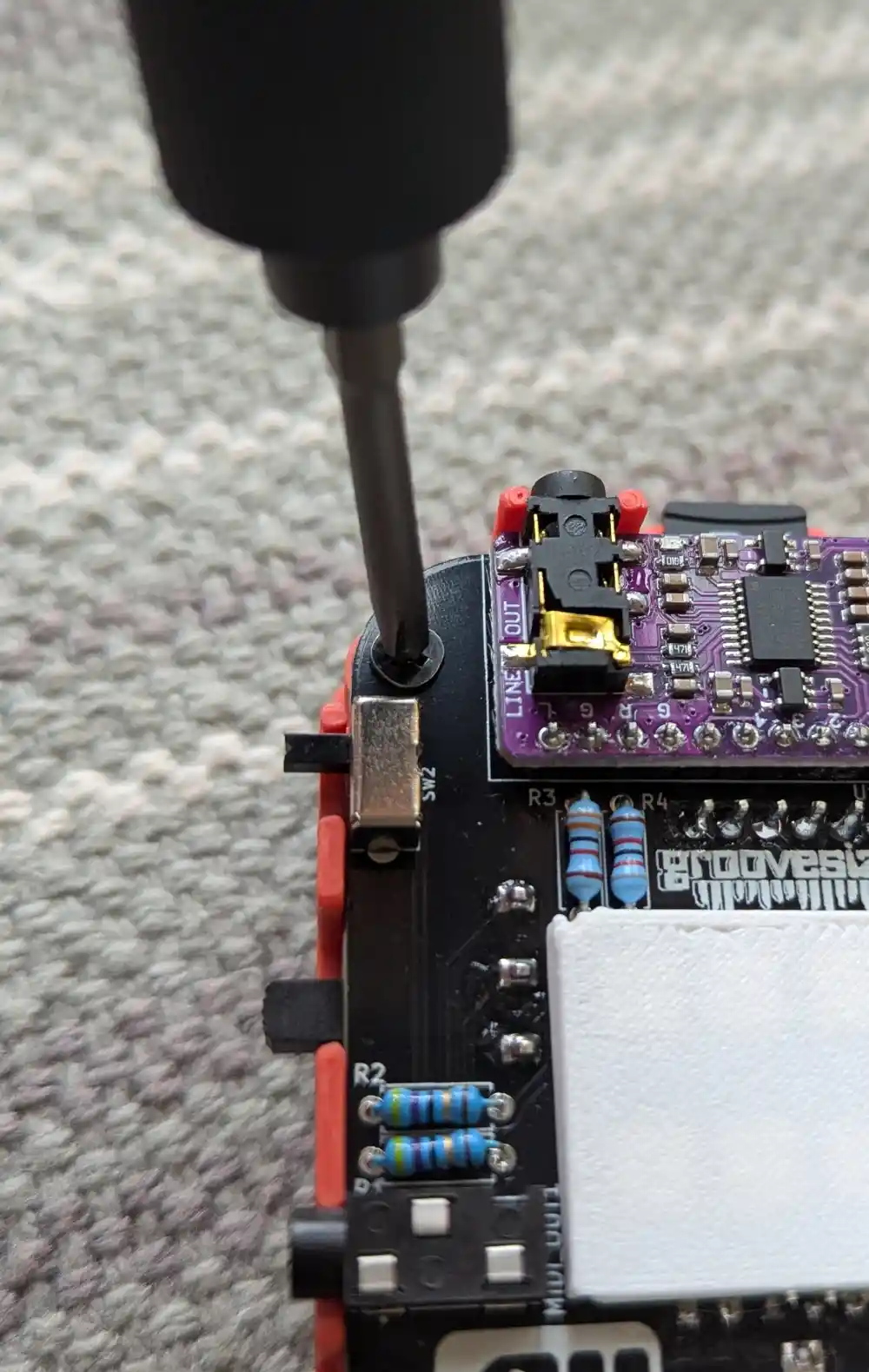
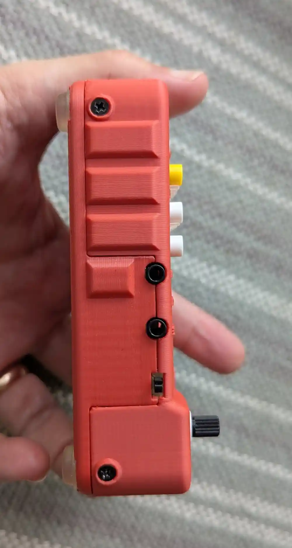
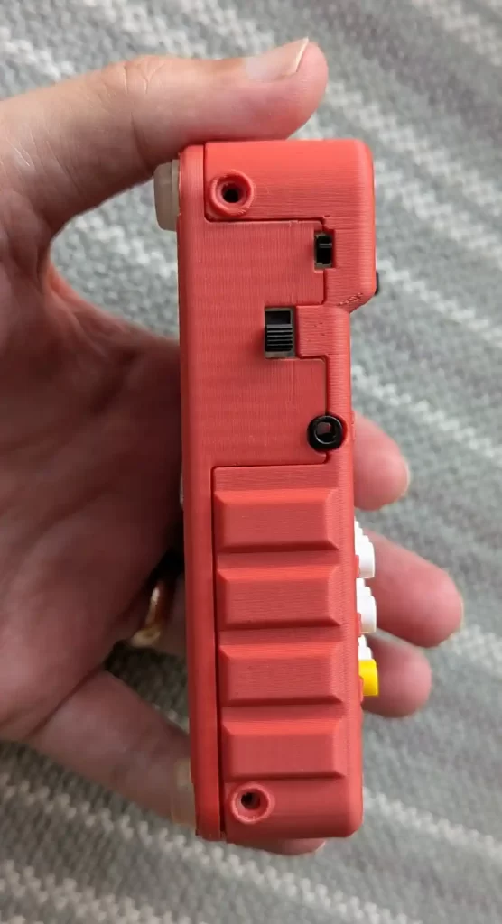
Now drop the top on, and screw in the 4 screws on the sides.
The view from the back.
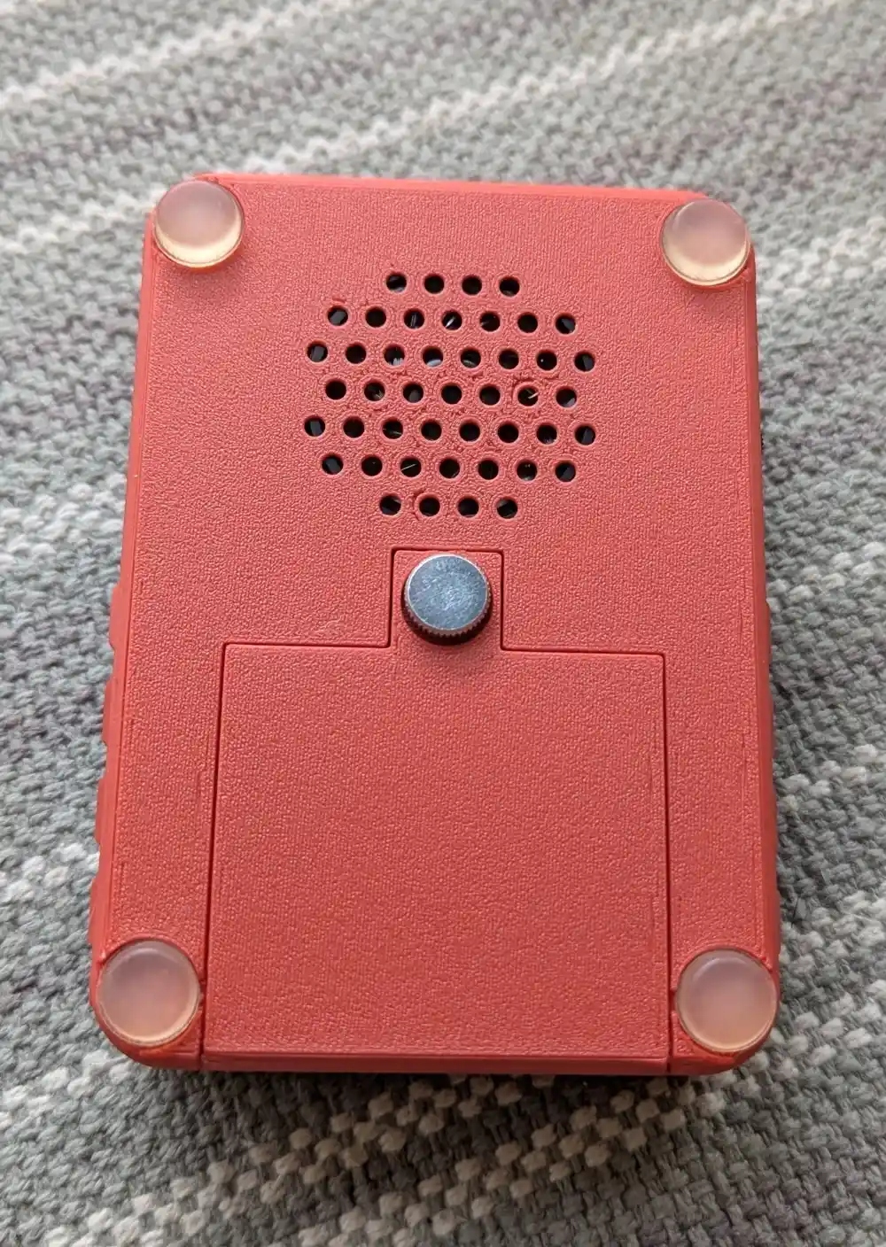
23.6 Enclosure (Cont.)
Finally, stick on the 4 bumper feet in the corners.
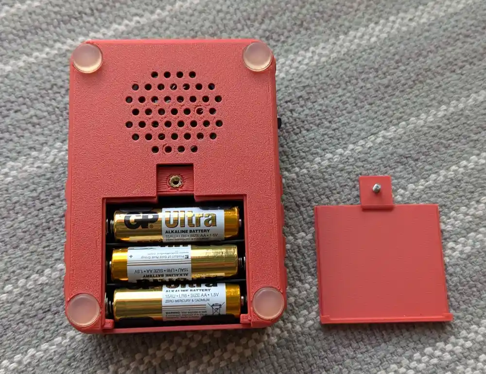
The view With the battery cover removed.
All done!
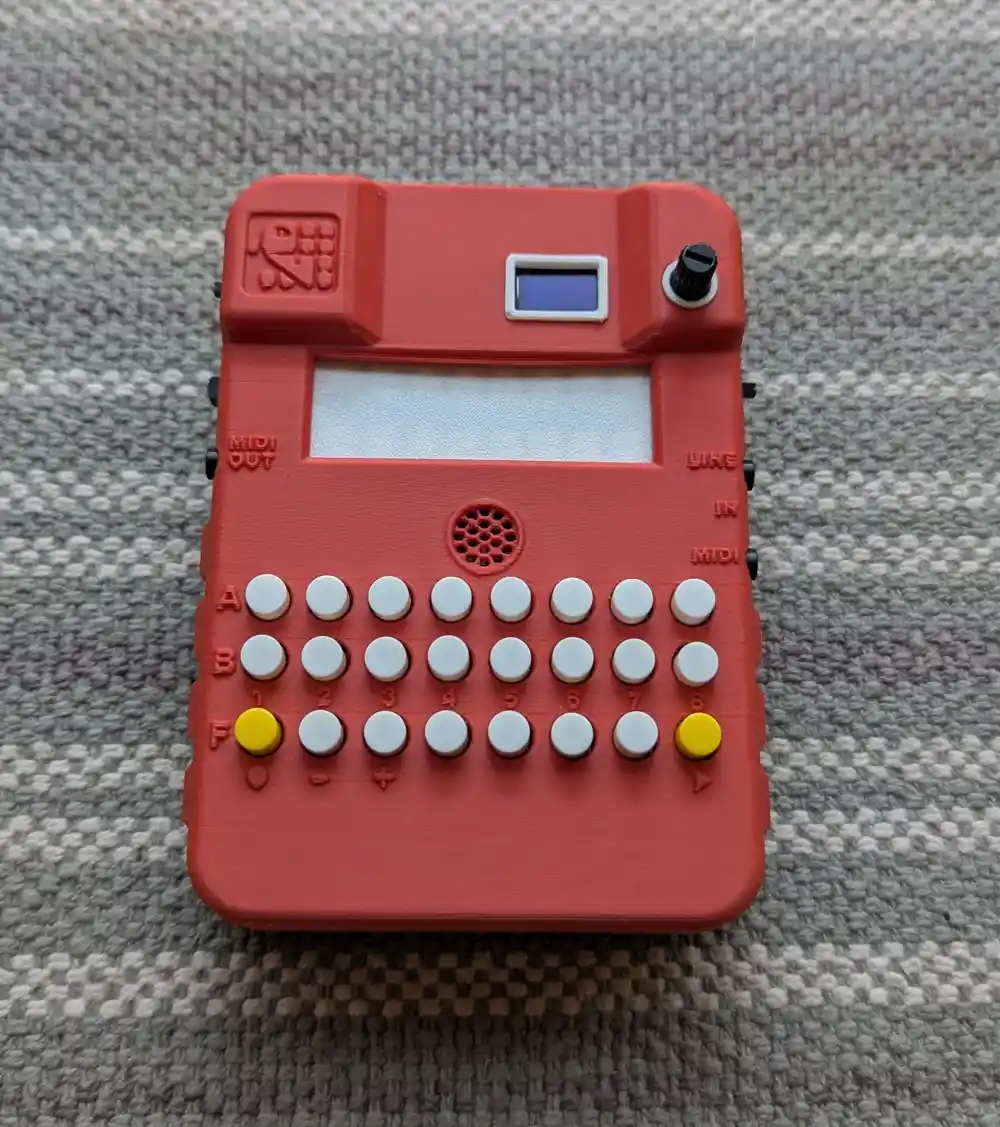
Congratulations, you’re done! Give yourself a big pat on the back.